Q.(a) Which of the following symbol represents a universal gate ?
You're viewing a preview — the full solution, concept, methods & PYQ mapping are locked.
Start your 14-day free trial to unlock the full solution →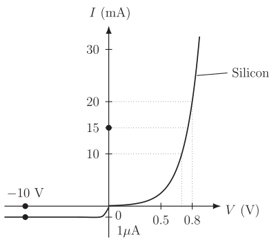
NAND (and, equivalently, NOR) is a universal logic gate; the described circuit is the standard set-up for the forward/reverse V–I characteristics of a p-n junction diode; and a common-emitter transistor amplifier's voltage gain works out to A_v = β·R_C/R_i.
(a) A universal gate is one from which any other logic gate (AND, OR, NOT, etc.) can be built using only that one type of gate. Both NAND and NOR have this property; NOT, OR/XOR and AND individually do not. Of the symbols listed, the NAND-gate symbol (a D-shaped gate with a small circle/bubble at its output, indicating the AND operation followed by inversion) is the universal gate. Answer: (ii).
(b)(i) The set-up described — a semiconductor diode with a voltmeter (V) connected across it to read the diode voltage, an ammeter (A) in series with it to read the diode current, and a battery with a key (plus typically a rheostat to vary the voltage) — is the standard circuit for the experiment to determine the current–voltage (V–I) characteristics of a p-n junction diode, done separately in forward bias and reverse bias configurations (by reversing the battery connections).
(ii) Resulting graph (I on the y-axis, V on the x-axis):
• Forward bias: as the forward voltage is increased from zero, the current stays extremely small until the applied voltage crosses a threshold or "knee" voltage (about 0.7 V for silicon, 0.3 V for germanium) — this is needed to overcome the junction's built-in potential barrier. Beyond the knee voltage, the current rises very steeply (almost exponentially) for a small further increase in voltage.
• Reverse bias: only a very small, almost constant reverse saturation current flows (of the order of µA, due to minority carriers), nearly independent of the reverse voltage — until the reverse voltage reaches the breakdown voltage, beyond which the current increases sharply.
The overall curve is therefore highly asymmetric/non-linear about the origin, confirming the diode's one-way (rectifying) conduction.
(c) Voltage gain of a transistor amplifier in common-emitter (CE) configuration: …
Unlock everything free for 14 days
- Full step-by-step solutions
- Concept-first explanations
- Methods, shortcuts & mistakes
- PYQ mapping + timed mock tests
Full access for 14 days. No credit card required.