Q.(a) Write the truth table for the combination of the gates shown in the figure.
🔒You're viewing a preview — the full solution, concept, methods & PYQ mapping are locked.
🔒 Start your 14-day free trial to unlock the full solution →Concept understanding — Logic Gate Truth Table
A truth table is the simplest way to show exactly what a logic gate does. Before you memorise any table, picture a light switch. The switch has two states: ON or OFF. In digital electronics, we call those states 1 (ON, high voltage) and 0 (OFF, low voltage). A logic gate is a tiny circuit that takes one or more of these 1/0 inputs and produces a single 1/0 output.
The truth table is just a complete list: for every possible combination of inputs, what output does the gate give? That's all. No hidden rules, no guesswork — it's the gate's entire behaviour written in a table.
The precise statement
A truth table for a logic gate is a tabular listing of all possible input combinations (in binary order) and the corresponding output for each combination. For a gate with n inputs, there are 2n rows.
Number of rows=2number of inputs
So a 2-input gate has 22=4 rows; a 3-input gate has 23=8 rows, and so on.
The simplest example: the NOT gate (inverter)
The NOT gate has only one input. It flips the signal: 1 becomes 0, 0 becomes 1.
| Input (A) | Output (Y) |
|---|---|
| 0 | 1 |
| 1 | 0 |
That's the truth table. Two rows, because 21=2. The output is always the opposite of the input.
A 2-input gate: the AND gate
The AND gate gives output 1 only when both inputs are 1. Otherwise, output is 0.
| Input A | Input B | Output Y=A⋅B |
|---|---|---|
| 0 | 0 | 0 |
| 0 | 1 | 0 |
| 1 | 0 | 0 |
| 1 | 1 | 1 |
Notice the pattern: the inputs are listed in binary counting order (00, 01, 10, 11). This is the standard way to write truth tables so you never miss a combination.
To quickly write any truth table, count in binary from 0 to 2n−1 for the inputs. That guarantees every combination appears exactly once.
Why this matters
A truth table is the definition of a logic gate. When you see a gate symbol (like the AND gate's D-shape), the truth table tells you exactly what it does. You don't need to guess or remember a vague description — the table is the complete, unambiguous behaviour.
For exam problems, you'll often be asked to:
- Write the truth table for a given gate
- Identify a gate from its truth table
- Combine gates and produce a truth table for the whole circuit
In every case, start with the inputs, list all 2n combinations in binary order, then work out the output for each row. That's the entire method.
One more example: the OR gate
The OR gate gives output 1 if at least one input is 1.
| A | B | Y=A+B |
|---|---|---|
| 0 | 0 | 0 |
| 0 | 1 | 1 |
| 1 | 0 | 1 |
Each first-stage NOR gate has both its inputs tied together, so it acts as a NOT gate (Aˉ and Bˉ); the third NOR of Aˉ,Bˉ gives Aˉ+Bˉ=A⋅B, i.e. an AND gate. …
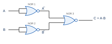
The network computes C=Aˉ+Bˉ=A⋅B (AND gate); photodiode = reverse-biased junction, light generates e–h pairs raising the reverse current.
(a) Combination of gates. Each of the two first NOR gates receives one input twice, so its output is the complement: Aˉ and Bˉ. The third NOR combines them:
C=Aˉ+Bˉ=Aˉˉ⋅Bˉˉ=A⋅B.
| A | B | Aˉ | Bˉ | C=A⋅B |
|---|---|---|---|---|
| 0 | 0 | 1 | 1 | 0 |
| 0 | 1 | 1 | 0 | 0 |
| 1 | 0 | 0 | 1 | 0 |
| 1 | 1 | 0 | 0 | 1 |
The combination behaves as an AND gate.
…
Showing the 12 most recent of 32 on this concept.
- AP EAPCET 2026Set eng-2026-05-12-FN1 markMCQQ.To have R = 1, values of A, B, C, D are respectively [circuit: inputs A and B feed a NAND gate; inputs C and D feed a second NAND gate; the outputs of both NAND gates feed an AND gate whose output is R] (A) 0, 1, 0, 0 (B) 1, 1, 1, 1 (C) 0, 1, 1, 1 (D) 1, 1, 0, 0
›Reveal solutionSolution
This tests reading a combinational logic diagram (two NAND gates feeding an AND gate) and checking which input combination yields the specified output. Answer: (A) 0, 1, 0, 0.
Concept and Intuition
A NAND gate outputs 1 unless both its inputs are 1 (it's 0 only when AB=1). Here, two NAND gates — one fed by A,B and one fed by C,D — feed a final AND gate producing R. For the final AND output R to be 1, both NAND outputs must individually be 1, which means neither AB nor CD can be the all-1s combination.
Step-by-Step Solution
- Logic: R=A⋅B ⋅ C⋅D.
- R=1 requires AB=1 (i.e. AB=11, so AB=0) AND CD=1 (i.e. CD=0).
- Test (A) A,B,C,D=0,1,0,0: AB=0×1=0⇒AB=1; CD=0×0=0⇒CD=1; R=1×1=1. ✓
- Test (B) 1,1,1,1: AB=1⇒AB=0; R=0. ✗ …
- AP EAPCET 2026Set eng-2026-05-12-AN1 markMCQQ.The truth table for the function of Y of A and B for the following logic gate (Figure: inputs A and B feed into an(OR)gate; the output of the(OR)gate feeds into one input of an AND gate; input A also feeds directly, via a separate line bypassing the(OR)gate, into the second input of the AND gate; the output of the AND gate is Y.) (A)(B)
A B Y 0 0 1 0 1 1 1 0 1 1 1 0 (C)A B Y 0 0 0 0 1 0 1 0 0 1 1 1 (D)A B Y 0 0 1 0 1 0 1 0 1 1 1 0 A B Y 0 0 0 0 1 0 1 0 1 1 1 1 ›Reveal solutionSolution
The AND gate combines (A OR B) with A itself; by the Boolean absorption law this simplifies to just Y=A, matching the truth table 0,0,1,1.
Concept and Intuition
The circuit computes Y=A⋅(A+B) (AND of A with the OR of A,B). This is a classic case of the Boolean absorption law, A⋅(A+B)=A: whenever A is true, the AND gate's other input (A+B) is automatically true too (since A+B is true whenever A is true), so the output just follows A. Whenever A is false, the AND output is false regardless of the other input, again matching A.
Step-by-Step Solution
- OR gate output: A+B.
- AND gate inputs: (A+B) and A (bypass line). Output: Y=A⋅(A+B).
- Case A=0,B=0: OR=0; Y=0⋅0=0.
- Case A=0,B=1: OR=1; Y=0⋅1=0.
- Case A=1,B=0: OR=1; Y=1⋅1=1.
- Case A=1,B=1: OR=1; Y=1⋅1=1. …
- AP EAPCET 2026Set eng-2026-05-14-AN1 markMCQQ.The given circuit consists of five logic gates. If the inputs are A = 0, B = 1, C = 1 and D = 0, then the outputs (y1, y2) are respectively [FIGURE: Gate 1 is a NAND gate with inputs A and B; Gate 2 is a NAND gate with inputs B and C; Gate 3 is an AND gate with inputs C and D; Gate 4 is an(OR)gate whose two inputs are the outputs of Gate 1 and Gate 2, producing output y1; Gate 5 is a NOR gate whose two inputs are the outputs of Gate 2 and Gate 3, producing output y2] (A) 1,1 (B) 1,0 (C) 0,1 (D) 0,0
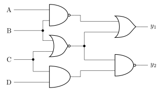
›Reveal solutionSolution
Propagate A=0,B=1,C=1,D=0 through the five gates: the NAND/OR path gives y1=1 and the NAND/AND/NOR path gives y2=1. Correct option: (A) 1,1.
Part (a)
Work from the primary inputs outward, computing each gate as soon as both its inputs are known.
NAND=A⋅B,AND=A⋅B,OR=A+B,NOR=A+B
- Gate 1 =A⋅B=0⋅1=0=1.
- Gate 2 =B⋅C=1⋅1=1=0. …
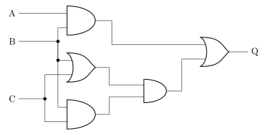
- AP EAPCET 2026Set eng-2026-05-18-FN1 markMCQQ.The value of Q in the given digital circuit is [FIGURE] (a digital logic circuit with three inputs A, B, C: A and B feed a top AND gate; B and C feed an OR gate; the OR gate's output together with C feed a middle AND gate; B and C also feed a bottom AND gate; the middle AND gate's output and the bottom AND gate's output feed into another AND gate; finally the top AND gate's output and this AND gate's output feed a final OR gate, whose output is Q) (A) Q=A+B+B.C(B+C) (B) Q=A.B+B.C(B+C) (C) Q=A+B+B.C(B.C) (D) Q=A.B+B.C(B+C)
›Reveal solutionSolution
Trace signals gate-by-gate through the circuit exactly as drawn (without pre-simplifying) to match the literal Boolean expression. Answer: Q=A.B+B.C(B+C).
Concept and Intuition
For a multi-gate digital logic diagram, the reliable method is to write the Boolean output of each gate in terms of its inputs, working left to right (or by signal flow), and substitute forward until you reach the final output. It's important to track the expression as the circuit builds it (even if it could be algebraically simplified later), since the answer choices here are given in un-simplified form matching the literal gate structure.
Step-by-Step Solution
- Gate 1 (AND, top): inputs A and B → output =A.B. This feeds straight into the final gate.
- Gate 2 (OR, second row): inputs tapped from the B and C lines → output =B+C.
- Gate 4 (AND, bottom row): inputs also tapped from the B and C lines → output =B.C.
- Gate 3 (small middle AND): combines Gate 2's output and Gate 4's output → output =(B+C).(B.C), written as B.C(B+C).
- Final gate (OR): combines Gate 1's output (A.B) and Gate 3's output (B.C(B+C)): Q=A.B+B.C(B+C).
Common Mistakes …
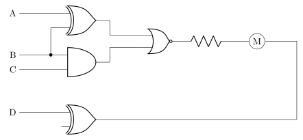
- AP EAPCET 2026Set ap-2026-05-19-FN1 markMCQQ.In the given logic circuit, the bulb will glow for which of the following combinations [FIGURE] (a logic circuit: inputs A goes into an XOR gate alone feeding one input of a NOR gate; inputs B and C go into a NAND gate feeding the other input of the NOR gate; the NOR gate output goes through a resistor to a bulb; input D goes into a separate XOR gate whose output forms the return path completing the circuit back to the bulb) (A) A=0,B=1,C=1,D=1 (B) A=1,B=0,C=0,D=0 (C) A=0,B=0,C=0,D=1 (D) A=1,B=1,C=1,D=0
›Reveal solutionSolution
The bulb is wired between the output of the top NOR gate and the output of the bottom XOR gate, so it glows exactly when those two outputs differ (are at opposite logic levels). Since the bottom XOR gate is drawn with only D as an explicit input, its unlabelled second input must be tied to logic 1 for the circuit to have a single well-defined answer (tying it to 0 makes three of the four options glow simultaneously, which cannot be right for a single-answer MCQ). With that resolved, only option (B) makes the bulb glow.
Concept and Intuition
The bulb sits in series between two different logic outputs — the top network's NOR output (Z) and the bottom XOR gate's output (W). Current flows through the bulb only when Z and W are at different logic levels (one HIGH, one LOW): Z ⊕ W = 1.
Step-by-step reasoning
-
Top network. X = A ⊕ B (top XOR), Y = NAND(B,C) = NOT(B·C), and Z = NOR(X,Y) = NOT(X+Y).
-
Bottom network. The bottom XOR gate's only labelled input is D. For the XOR to behave as a definite function of D alone, its second input must be tied to a fixed logic level. Tying it to 0 gives W = D ⊕ 0 = D — but checking all four options under this assumption makes (A), (C), and (D) all glow, which is impossible for a single-answer question. Tying the second input to logic 1 gives W = D ⊕ 1 = D̄ (an inverter), and this is the only assumption that yields exactly one glowing option.
-
Bulb condition. With W = D̄, the bulb glows when Z ≠ D̄, i.e., when Z = D.
-
Check each option (Z = D required to glow): …
-
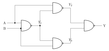
- AP EAPCET 2026Set eng-2026-05-18-AN1 markMCQQ.In the logic circuit, if A=1 and B=1, the outputs Y3 and Y are respectively [FIGURE] (a logic circuit: inputs A and B feed into a NAND gate producing output Y1; Y1 together with a feedback line from input A feed into a second NAND gate producing output Y2; Y1 together with a feedback line from input B feed into a third NAND gate producing output Y3; Y2 and Y3 feed into a final NAND gate whose output is Y) (A) 0,0 (B) 0,1 (C) 1,0 (D) 1,1
›Reveal solutionSolution
This four-NAND arrangement is the classic NAND-only XOR gate; working the gates through in order for A=B=1 gives Y3=1 and the final output Y=0.
Concept and Intuition
A 2-input NAND gate outputs 0 only when both inputs are 1; otherwise it outputs 1. Building an XOR from four NAND gates is a standard digital-logic construction: the first NAND combines A,B; two more NANDs each combine that result with one of the original inputs; the last NAND combines those two outputs. The overall behaviour reproduces Y=A⊕B. Rather than relying on that fact from memory, we can just propagate the logic level through gate by gate, which is the reliable and rigorous way to solve it.
Step-by-Step Solution
- Y1=A⋅B=1⋅1=1=0.
- Y2=A⋅Y1=1⋅0=0=1.
- Y3=B⋅Y1=1⋅0=0=1. …
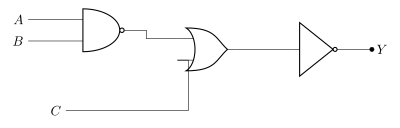
- AP EAPCET 2026Set ap-2026-05-20-FN1 markMCQQ.For the circuit given below, which of the following is correct option? [FIGURE] (a logic-gate circuit: inputs A and B feed into a NAND gate; the NAND gate's output together with input C feed into an OR gate; the OR gate's output feeds into a NOT gate whose output is Y) (A) A=B=1,C=0⇒Y=0 (B) A=B=1,C=0⇒Y=1 (C) A=B=0,C=1⇒Y=1 (D) A=B=C=1⇒Y=1
›Reveal solutionSolution
This is a logic-gate truth-table evaluation: NAND(A,B) feeds an OR gate with C, whose output is inverted to give Y.
Concept and Intuition
Build the compound Boolean expression Y=(A⋅B)′+C... more precisely Y=NOT(NAND(A,B) OR C), then evaluate it for each option's input combination and check which one produces the stated output.
Step-by-Step Solution
- Let N=NAND(A,B)=A⋅B, O=N+C (OR), and Y=O (NOT).
- Test A=B=1,C=0: N=1⋅1=1=0. O=0+0=0. Y=0=1. → matches option (B)'s claim of Y=1.
- Test A=B=0,C=1 (option C's claim of Y=1): N=0=1. O=1+1=1. Y=1=0 — contradicts option (C). …
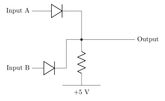
- AP EAPCET 2026Set ap-2026-05-20-AN1 markMCQQ.[FIGURE] (a circuit with Input A and Input B each passing through a diode oriented toward a common output node; the output node is also connected through a resistor to +5 V) The following circuit represents the logic gate (A) AND gate (B)(OR)gate (C) NOR gate (D) NAND gate
›Reveal solutionSolution
The diode-resistor combination with an inverting output stage gives an output that is LOW only when both inputs are HIGH — the truth table Y=A⋅B. Correct option: (D) NAND gate.
Part (a)
In a diode logic gate, diodes act as switches and the resistor sets the resting level of the output node. Here the two inputs connect to a common node through diodes and the node is pulled to +5V through a resistor; the following inverting (transistor) stage complements the result. The net behaviour is that the output is HIGH except when every input is HIGH, which is the NAND function.
Y=A⋅B …
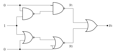
- AP EAPCET 2025Set eng-2025-05-21-AN1 markMCQQ.If five logic gates are connected as shown in the figure, then the values of y1, y2 and y3 are respectively [FIGURE] (a logic-gate network: inputs 0 (top), 1 (middle), 0 (bottom); the top and middle inputs feed a NAND gate whose output, together with the top input fed forward, feeds a second NAND gate producing y1; the middle and bottom inputs feed a NOR gate whose output, together with the bottom input fed forward, feeds a second NOR gate producing y2; y1 and y2 feed a final(OR)gate producing y3) (A) 1, 1, 1 (B) 0, 0, 1 (C) 1, 1, 0 (D) 1, 0, 1
›Reveal solutionSolution
With inputs 0,1,0 the NAND path gives y1=1, the NOR path gives y2=1, and the final OR gives y3=1. Correct option: (A) 1,1,1.
Part (a)
Evaluate each gate in the order the signals flow; the fed-forward original input line is one input of the second gate in each branch.
NAND=A⋅B (0 only when both 1),NOR=A+B (1 only when both 0)
Inputs (top, middle, bottom) =(0,1,0).
- Gate 1 (NAND of top, middle): 0⋅1=0=1.
- Gate 2 (NAND of top and Gate 1): 0⋅1=0=1=y1.
- Gate 3 (NOR of middle, bottom): 1+0=1=0. …
- AP EAPCET 2025Set eng-2025-05-23-FN1 markMCQQ.The logic gate equivalent to the circuit shown in the figure is [FIGURE] (a circuit with inputs A and B fed into an(OR)gate, whose output feeds both inputs of an AND gate, whose output feeds a NOT (inverter) gate, producing output y) (A) AND (B) NAND (C) NOR (D)(OR)

›Reveal solutionSolution
An OR feeding an AND gate whose two inputs are the same signal (P⋅P=P) followed by a NOT reduces to an inverted OR, i.e. a NOR gate. Correct option: (C) NOR.
Part (a)
A useful simplification: any gate fed the same signal on both inputs acts as a buffer, since P⋅P=P and P+P=P.
- OR gate: P=A+B.
- AND gate with both inputs =P: output =P⋅P=P=A+B.
- NOT gate: y=P=A+B. …
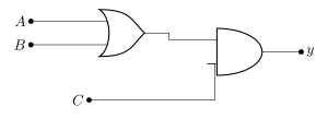
- AP EAPCET 2025Set ap-2025-05-20-FN1 markMCQQ.To get an output value 1 from the given circuit, the input values of A, B and C are [FIGURE] (a logic circuit diagram: inputs A and B feed into an(OR)gate; the output of the(OR)gate, together with input C, feeds into an AND gate whose output is y) (A) 0, 1, 0 (B) 0, 0, 1 (C) 1, 0, 1 (D) 1, 0, 0
›Reveal solutionSolution
The circuit is y=AND(OR(A,B),C); for y=1 we need C=1 and at least one of A,B true — only option (C), A=1,B=0,C=1, satisfies this.
Concept and Intuition
An AND gate outputs 1 only when all its inputs are 1; an OR gate outputs 1 when at least one input is 1. Here the OR gate combines A and B, and its output feeds into the AND gate along with C. So the overall output is y=(A+B)⋅C in Boolean notation.
Step-by-Step Solution
- Write the output logically: y=(A OR B) AND C.
- For y=1: need C=1 AND (A=1 or B=1).
- Test option (A) 0,1,0: A+B=1, but C=0⇒y=0. Fails.
- Test option (B) 0,0,1: A+B=0⇒y=0. Fails. …
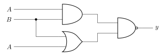
- AP EAPCET 2025Set eng-2025-05-23-AN1 markMCQQ.If three logic gates are connected as shown in the figure, then the correct truth table of the circuit is [FIGURE] (three logic gates: inputs A and B feed a two-input AND gate; inputs B and A feed a two-input(OR)gate; the outputs of the AND gate and the(OR)gate feed a two-input NAND gate whose output is y) (A) A=0,B=0 -> y=1; A=0,B=1 -> y=0; A=1,B=0 -> y=0; A=1,B=1 -> y=1 (B) A=0,B=0 -> y=1; A=0,B=1 -> y=1; A=1,B=0 -> y=1; A=1,B=1 -> y=0 (C) A=0,B=0 -> y=0; A=0,B=1 -> y=0; A=1,B=0 -> y=0; A=1,B=1 -> y=1 (D) A=0,B=0 -> y=0; A=0,B=1 -> y=1; A=1,B=0 -> y=1; A=1,B=1 -> y=0
›Reveal solutionSolution
The circuit simplifies to a plain NAND(A,B): combining an AND and an OR gate feeding a final NAND collapses algebraically to y=A⋅B, so y is 0 only when A=B=1.
Concept and Intuition
When the output of an AND gate and the output of an OR gate (both fed the same two inputs A,B) are combined through a NAND gate, Boolean algebra lets us simplify the whole thing to a single familiar gate. This is a common 'disguised gate' question — the point is to not be intimidated by three gates and instead reduce it symbolically.
Step-by-Step Solution
- Let the AND gate output be P=A⋅B.
- Let the OR gate output be Q=A+B.
- The final gate is a NAND of P and Q: y=P⋅Q=(A⋅B)⋅(A+B).
- Simplify (A⋅B)⋅(A+B): whenever A⋅B=1 (i.e., both A=1,B=1), A+B is automatically 1 too. So (A⋅B)(A+B)=A⋅B always (absorption law).
- Hence y=A⋅B, i.e., a NAND gate on A and B. …
🎓Unlock everything free for 14 days
- ✓Full step-by-step solutions
- ✓Concept-first explanations
- ✓Methods, shortcuts & mistakes
- ✓PYQ mapping + timed mock tests
Full access for 14 days. No credit card required.