Q.With the help of a circuit diagram, explain the working of a p-n junction diode as a full-wave rectifier. Also draw its input and output waveforms.
You're viewing a preview — the full solution, concept, methods & PYQ mapping are locked.
Start your 14-day free trial to unlock the full solution →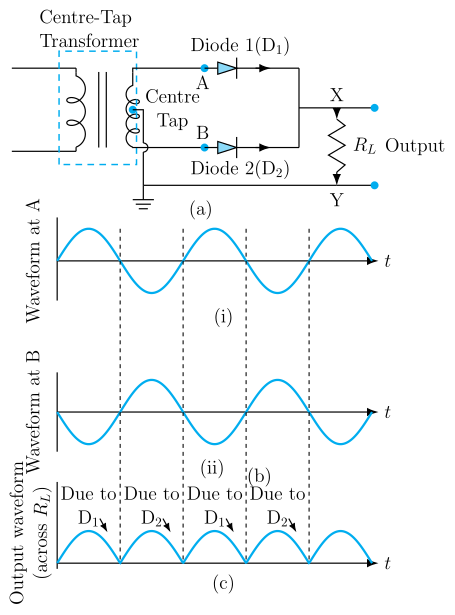
A full-wave rectifier uses two diodes and a centre-tapped transformer to convert both halves of an AC input into a unidirectional output. The key idea: during each half-cycle, one diode conducts while the other is reverse-biased, so current always flows through the load in the same direction. The output has a much smaller ripple than a half-wave rectifier.
Why Full-Wave Rectification?
A p-n junction diode allows current to flow only when forward-biased (p-side at higher potential than n-side). In a half-wave rectifier, only one half of the AC cycle is used — the other half is wasted. A full-wave rectifier fixes this by using both halves of the input waveform.
The trick is to use a centre-tapped transformer — a transformer whose secondary winding has a tap exactly at its midpoint. This gives us two equal AC voltages that are out of phase with each other. With two diodes, we can steer current from both halves of the cycle through the load in the same direction.
Step-by-Step Working
1. The Circuit Setup
The circuit consists of:
- A centre-tapped transformer (step-down, typically)
- Two identical p-n junction diodes, D₁ and D₂
- A load resistor
Picture the secondary winding of the transformer with its two outer ends labelled A and B, and its exact midpoint tapped at CT. The anode of diode D₁ connects to end A, and the anode of diode D₂ connects to end B. The cathodes of both diodes are joined together at one common point, which forms one terminal of the load resistor ; the other terminal of connects back to the centre tap CT. With this arrangement, whichever diode happens to be conducting at a given instant, current always flows from the common cathode junction, through , and back to the centre tap — in the same direction every time.
2. During the Positive Half-Cycle
Let the voltage at A be positive with respect to the centre tap CT. Then:
- A is at , B is at (since B is out of phase)
- Diode D₁: anode at A (positive), cathode at the common point → forward-biased → conducts
- Diode D₂: anode at B (negative), cathode at common point → reverse-biased → does not conduct
Current flows: A → D₁ → → CT. The voltage across is positive (top end positive with respect to bottom).
3. During the Negative Half-Cycle
Now A goes negative and B goes positive with respect to CT:
- A is at , B is at
- D₁ is reverse-biased (anode negative) → does not conduct
- D₂ is forward-biased (anode positive) → conducts
Current flows: B → D₂ → → CT. Notice: current through still flows from top to bottom — the same direction as before.
The key insight: even though the input alternates, the load current always flows from the common cathode junction to the centre tap. The diodes take turns “handing off” the current every half-cycle.
4. The Output Waveform
The input to each diode is a half-wave of the AC signal. But because they conduct on alternate half-cycles, the output across consists of both halves of the input, all rectified to the same polarity. …
Unlock everything free for 14 days
- Full step-by-step solutions
- Concept-first explanations
- Methods, shortcuts & mistakes
- PYQ mapping + timed mock tests
Full access for 14 days. No credit card required.