Electronics · Ch 1 — Field Effect Transistor (FET)
Introduction to the Field Effect Transistor
Introduction to the Field Effect Transistor
A field effect transistor (FET) is a three-terminal, unipolar solid-state device in which the current is controlled by an electric field. Unlike the bipolar junction transistor (BJT), where conduction relies on both majority and minority carriers, an FET conducts using majority carriers only — either electrons or holes — which is exactly what the word unipolar means. FETs are used across a wide range of applications, from small-signal amplifiers to switching in integrated circuits.
Classification of FETs
FETs fall into two main families:
- Junction FET (JFET) — the gate is an ordinary reverse-biased pn junction.
- Metal-oxide semiconductor FET (MOSFET), also called the Insulated Gate FET (IGFET) — the gate is separated from the channel by a thin insulating oxide layer.
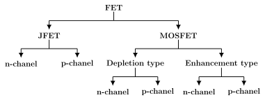
Depending on its structure, a JFET is further divided into the n-channel JFET and the p-channel JFET. The full classification, from the FET root down to the n- and p-channel leaves of the JFET and the depletion- and enhancement-type MOSFETs, is shown in Figure 1.1.1.
How the FET differs from the BJT. The FET is a voltage-controlled device — its output current is set by varying the input voltage — whereas the BJT is a current-controlled device whose output current is set by varying the input current. Conduction in an FET is by majority carriers only (holes or electrons), so it is unipolar; in a BJT both majority and minority carriers take part, making it bipolar. FETs come as n-channel or p-channel types, while BJTs come as npn or pnp types. The two devices also share features: each has three terminals and two pn junctions.
Construction of the JFET
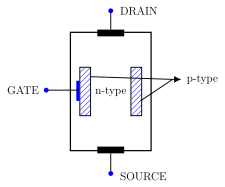
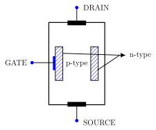
An n-channel JFET (Figure 1.1.2a) is built from a bar of n-type semiconductor. Two heavily doped p-type regions are diffused into opposite sides of the bar, forming two pn junctions facing each other across the bar. The strip of n-type material lying between these two junctions is called the channel, and it is the path through which the charge carriers flow. The two p-type regions are joined internally and brought out as a single terminal, the gate. Two ohmic (non-rectifying) contacts are made to the ends of the bar and named the drain and the source. A p-channel JFET (Figure 1.1.2b) is the mirror image: a p-type channel with two n-type gate regions on its sides, and the same drain, source and gate terminals.
The terminals of the JFET
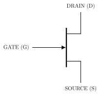
The schematic symbols are shown in Figure 1.1.3a (n-channel) and Figure 1.1.3b (p-channel); the vertical line stands for the channel, and the direction of the gate arrow distinguishes the two types — for the n-channel type the arrow points towards the channel line, and for the p-channel type it points away from it. The three terminals do the following jobs:
- Source (S) — supplies the charge carriers that take part in conduction.
- Drain (D) — collects the charge carriers delivered by the source.
- Gate (G) — controls the flow of carriers through the channel when a suitable potential is applied to it.
When a suitable voltage is applied across the drain and source, carriers travel from source to drain and constitute the device current. The key distinction from a BJT is that BJT current involves both types of charge carrier (electrons and holes), whereas the JFET current is carried by majority carriers alone.
Formation of the depletion region
Consider an n-channel JFET. The pn junctions formed between the n-type channel and the p-type gate regions are always reverse biased during normal operation. A gate supply reverse biases both junctions. Under reverse bias, electrons and holes diffuse away from the junction, leaving behind immobile positive ions on the n-side and immobile negative ions on the p-side. This layer of immobile ions, empty of free carriers, is the depletion region (Figure 1.1.4). Its thickness grows as the reverse-bias voltage is increased.
How far the depletion region spreads depends on the doping: it extends more into the lightly doped side. Because the p-type gate of an n-channel JFET is heavily doped compared with the n-type channel, the depletion region reaches further into the n-channel.
Reverse bias is also produced by the drain supply connected across source and drain (Figure 1.1.5), which makes the drain positive with respect to the source and so reverse biases the gate-source junction. The n-channel between source and drain behaves like two variable resistors and in series (Figure 1.1.6), whose values depend on and . With the gate left open, drives electrons from source to drain, constituting the drain current (conventional current flows drain to source). This drain current produces a voltage drop across that reverse biases the gate-to-source junction, so a depletion region forms inside the channel even when the gate is open-circuited. The depletion region is not symmetric — it bulges more towards the drain and less towards the source, because the voltage drop across (nearer the drain) is greater than that across (nearer the source).
Working of the n-channel JFET
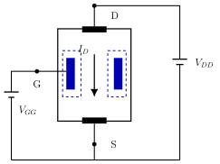
With both the gate-source supply and the drain-source supply connected (Figure 1.1.7), the reverse bias pushes the depletion regions further into the channel. When (gate open), the drain current is a maximum and flows from drain to source; this maximum value is the drain-source saturation current . As is increased, the reverse bias across the junctions grows, the channel narrows, and the drain current falls. Increasing the reverse bias still further widens the depletion regions and reduces more — so the device current is controlled mainly by the reverse voltage applied across the gate and source.
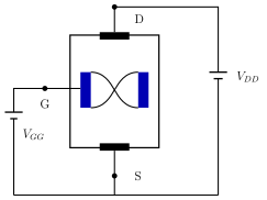
When is made large enough, a stage is reached where the two depletion regions touch each other (Figure 1.1.8) and completely block the channel, so the drain current falls to zero. The gate voltage at which the drain current becomes zero is called the pinch-off voltage ; it depends on the doping level and the channel width. The p-channel JFET works in exactly the same way, except that the current carriers are holes and the polarities of and are reversed.
Characteristics of the n-channel JFET
A JFET has two main sets of characteristic curves:
- (a) Drain characteristics — the curves relating the drain current to the drain-to-source voltage at a constant gate-to-source voltage .
- (b) Transfer characteristics — the curves relating the drain current to the gate-to-source voltage at a constant drain-to-source voltage .
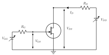
Both are obtained from the test circuit of Figure 1.1.9, in which sets the gate-source voltage through and sets the drain-source voltage through .
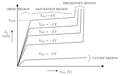
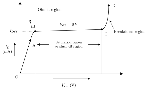
Drain characteristics. With first set to zero, is noted for various and plotted with on the x-axis and on the y-axis (Figure 1.1.10); the maximum current on the curve is . Repeating for several gate voltages () gives a family of curves. Looking at the curve in detail (Figure 1.1.11), four regions appear:
- Ohmic region (OA): rises almost proportionally with because the n-channel behaves like a resistor.
- Pinch-off / saturation region (AB–BC): past the knee at A, increases only slowly as the expanding depletion region reduces the channel; pinch-off occurs when the channel is fully blocked at , and along BC the drain current stays essentially constant at its maximum value. Here and obey Shockley's equation.
- Breakdown region (CD): beyond C the drain current shoots up rapidly with because of the avalanche effect.
[!NOTE] The textbook prints Shockley's equation as “Schokley's equation” — a spelling slip in the source. The relation and its physics are unchanged; the standard name is Shockley's equation.
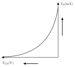
Transfer (transconductance) characteristics. The transconductance curve gives the relation between and at a constant (Figure 1.1.12). Using the circuit of Figure 1.1.9, is held at a fixed value such as 4 V, is recorded for different , and is plotted against . The curve obeys the same Shockley relation , where is the pinch-off voltage: is near zero at large negative (near pinch-off) and rises to as approaches zero.
JFET parameters
Four important parameters are read from the characteristic curves:
- DC drain resistance — the ohmic resistance, the ratio of to at constant , measured in ohm. (The book names it in the text but writes the symbol in the formula box — the same quantity.)
- AC drain resistance — also called the dynamic drain resistance, the ratio of a small change in to the resulting change in at constant , in ohm. …
Drawn by us to help you understand the concept clearly, and verified to make sure it's accurate. For exams, practice from your textbook's own diagram.
A downward hierarchical tree (Figure 1.1.1) showing how FETs are classified. The FET root splits into JFET and MOSFET; the JFET splits into n-channel and p-channel types, and the MOSFET splits into depletion-type and enhancement-type, each of which again splits into n-channel and p-channel. It gives the student the whole family map at a glance before the individual devices are studied. (The book's l …
A three-terminal, unipolar solid-state device in which the current between the drain and source is controlled by the electric field produced by a voltage applied to the gate. Because conduction is by majority carriers only, it is cal …
Drawn by us to help you understand the concept clearly, and verified to make sure it's accurate. For exams, practice from your textbook's own diagram.
Figure 1.1.2a shows the construction of an n-channel JFET: a central n-type semiconductor bar with an ohmic contact at the top leading to the DRAIN terminal and one at the bottom leading to the SOURCE terminal, and two heavily doped p-type gate regions on the left and right inner edges (joined to a single GATE terminal). The n-type strip between the two p-regions is the channel. It matters bec …
Drawn by us to help you understand the concept clearly, and verified to make sure it's accurate. For exams, practice from your textbook's own diagram.
Figure 1.1.2b shows the construction of a p-channel JFET — a central p-type bar with DRAIN and SOURCE ohmic contacts and two n-type gate regions on its sides brought out as the GATE. It is the material-swapped mirror of Figure 1.1.2a and helps the student see that both JFET types share the same lay …
The region of semiconductor between the two gate pn junctions of a JFET through which the charge carriers flow from source to drain. In an n-channel JFET the channel is n-type; i …
Drawn by us to help you understand the concept clearly, and verified to make sure it's accurate. For exams, practice from your textbook's own diagram.
Figure 1.1.3a is the schematic symbol of the n-channel JFET: a vertical line for the channel with the drain (D) at the top, source (S) at the bottom and a horizontal gate (G) lead whose arrowhead points TOWARDS the channel line. The arrow direction is the quick visual test tha …
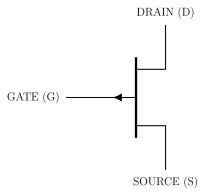
Drawn by us to help you understand the concept clearly, and verified to make sure it's accurate. For exams, practice from your textbook's own diagram.
Figure 1.1.3b is the schematic symbol of the p-channel JFET: the same channel line with drain (D), source (S) and gate (G), but the gate arrowhead points AWAY from the channel line — the opposite of th …
The layer of immobile positive and negative ions, empty of free charge carriers, that forms on either side of a reverse-biased pn junction. In a JFET the gate junctions are always reverse biased, so depletion regions grow into the channel and narrow the conducting path; the …
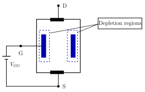
Drawn by us to help you understand the concept clearly, and verified to make sure it's accurate. For exams, practice from your textbook's own diagram.
Figure 1.1.4 shows an n-channel JFET whose gate is reverse biased by the supply ; dashed depletion regions surround the two p-type gate regions and a callout labels them 'Depletion regions'. It illustrates how gate reverse bias alone sets up t …
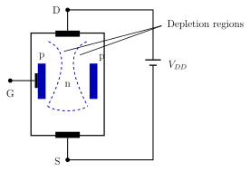
Drawn by us to help you understand the concept clearly, and verified to make sure it's accurate. For exams, practice from your textbook's own diagram.
Figure 1.1.5 shows the depletion regions produced when the drain supply makes the drain positive with respect to the source. The curved dashed boundaries bulge more towards the drain (top) and narrow towards the source (bottom), showing the asymmetry caused by the larg …
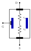
Drawn by us to help you understand the concept clearly, and verified to make sure it's accurate. For exams, practice from your textbook's own diagram.
Figure 1.1.6 models the n-channel between drain and source as two variable resistors in series — nearer the drain and nearer the source — whose values depend on and . It explains why the drain current develops a drop across that reverse biase …
Drawn by us to help you understand the concept clearly, and verified to make sure it's accurate. For exams, practice from your textbook's own diagram.
Figure 1.1.7 is the complete operating circuit of the n-channel JFET: the gate is reverse biased by on the left, the drain supply is connected across drain and source on the right, and an arrow inside the channel marks the drain current . It ties the const …
The gate-to-source voltage at which the two depletion regions in the channel just meet and completely block it, so that the drain current falls to zero. Its value depends on the dop …
Drawn by us to help you understand the concept clearly, and verified to make sure it's accurate. For exams, practice from your textbook's own diagram.
Figure 1.1.8 shows the JFET at pinch-off: the two curved depletion boundaries touch in the centre of the channel, completely blocking it so the drain current becomes zero. It is the visual anchor for the def …
The maximum drain current that flows in a JFET when the gate-to-source voltage is zero (, gate open). It is the reference current in Shockley's equation and marks the top of …
Drawn by us to help you understand the concept clearly, and verified to make sure it's accurate. For exams, practice from your textbook's own diagram.
Figure 1.1.9 is the measurement circuit used to obtain both the drain and transfer characteristics. A variable supply sets the gate-source voltage through , and a variable supply sets the drain-source voltage through , while is read in the drain branch. It is the c …
Drawn by us to help you understand the concept clearly, and verified to make sure it's accurate. For exams, practice from your textbook's own diagram.
Figure 1.1.10 is the family of drain characteristics: plotted against for . Each curve rises through an ohmic region, flattens into a saturation region, and turns sharply upward in the breakdown region; the plateau of the top () curve marks . It shows how the gate voltage sets the current level. (The printed caption …
Drawn by us to help you understand the concept clearly, and verified to make sure it's accurate. For exams, practice from your textbook's own diagram.
Figure 1.1.11 is the drain curve drawn on its own with the key points labelled: it climbs steeply through the ohmic region to A, bends at the knee to B (plateau level ), runs almost flat through the saturation/pinch-off region to C, then rises sharply to D in the breakdown region. I …
The drain current in the pinch-off (saturation) region in terms of the drain-source saturation current , the gate-source voltage $V_{GS} …
Drawn by us to help you understand the concept clearly, and verified to make sure it's accurate. For exams, practice from your textbook's own diagram.
Figure 1.1.12 is the transconductance (transfer) curve: on the vertical axis against drawn in the negative (leftward) direction. is near zero at large negative (close to pinch-off) and rises steeply to its maximum as approaches zero, …
The ohmic (DC) drain resistance, in ohm. The book names this parameter in the text but writes the symbol i …
The ratio of a small change in drain-source voltage to the resulting change in drain current, in ohm; also ca …
The ratio of a small change in drain current to the change in gate-source voltage that produced it, measured in siemen (S); also …
A pure number giving the ratio of a small change in drain-source voltage to the corresponding change in gate-source …
The amplification factor equals the product of the AC drain resistance and the transconductance, obtained from by inserting …
Obtained by differentiating Shockley's equation with respect to ; is the …
| Sl no | FET | BJT |
|---|---|---|
| 1 | It is a unipolar device. | It is a bipolar device. |
| 2 | Current conduction is only by majority charge carriers i.e., either holes or electrons. | Current conduction is by both the charge carriers (majority & minority carriers) i.e., both holes & electrons. |
| 3 | It is a voltage controlled device. | It is a current controlled device. |
| 4 | Input resistance is very high, in the order of several mega ohm. | Input resistance is very low, i.e., in the order of few kilo ohm. |
| 5 | It has high switching speed. | It has low switching speed. |