Physics · Ch 14 — Semiconductor Electronics: Materials, Devices and Simple Circuits
Classification of Metals, Conductors and Semiconductors
Classification of Metals, Conductors and Semiconductors
14.2 Classification of Metals, Conductors and Semiconductors
Classification Based on Electrical Conductivity
Solids are broadly divided into three categories based on their electrical conductivity or resistivity .
Metals have very low resistivity (high conductivity). Typical ranges are:
Semiconductors have resistivity or conductivity intermediate between metals and insulators:
Insulators have high resistivity (low conductivity):
These ranges are indicative — actual values for a given material may fall outside these limits. Resistivity alone is not the sole criterion for classification; other differences will emerge as we study semiconductors further.
Types of Semiconductors
Semiconductors are classified by composition:
Elemental semiconductors: Silicon (Si) and Germanium (Ge).
Compound semiconductors:
- Inorganic compounds: CdS, GaAs, CdSe, InP, and others.
- Organic compounds: anthracene, doped phthalocyanines, and similar materials.
- Organic polymers: polypyrrole, polyaniline, polythiophene, and related polymers.
Most commercially available semiconductor devices today are based on elemental semiconductors Si or Ge, or on inorganic compound semiconductors. Since the 1990s, devices using organic semiconductors and semiconducting polymers have emerged, signalling the birth of polymer electronics and molecular electronics. This chapter focuses on inorganic semiconductors — primarily Si and Ge — but the general concepts introduced here apply broadly to most compound semiconductors as well.
Classification Based on Energy Bands
From Isolated Atoms to Energy Bands
In an isolated atom, each electron's energy is determined by the orbit it occupies, as described by the Bohr model. When atoms come together to form a solid, they are packed closely. The outer orbits of electrons from neighbouring atoms come very close together — they may even overlap. This proximity fundamentally changes the nature of electron motion compared to an isolated atom.
Inside a crystal, each electron occupies a unique position, and no two electrons experience exactly the same pattern of surrounding charges. Consequently, each electron has a different energy level. These many different energy levels, varying continuously, form what are called energy bands.
Valence Band and Conduction Band
The energy band that contains the energy levels of the valence electrons is called the valence band. The energy band immediately above the valence band is called the conduction band.
With no external energy supplied, all valence electrons reside in the valence band. The conduction band is normally empty.
If the lowest energy level in the conduction band happens to be lower than the highest level of the valence band, electrons from the valence band can easily move into the conduction band. This is the situation when the bands overlap — the case for metallic conductors.
If there is a gap between the conduction band and the valence band, electrons in the valence band remain bound, and no free electrons are available in the conduction band. This makes the material an insulator. However, some electrons from the valence band may gain enough external energy to cross this gap and enter the conduction band. When they do, they create vacant energy levels in the valence band where other valence electrons can move. This creates the possibility of conduction both by electrons in the conduction band and by vacancies (holes) in the valence band.
Energy Bands in Silicon and Germanium
Consider a crystal of Si or Ge containing atoms. For Si, the outermost orbit is the third orbit (); for Ge, it is the fourth orbit (). Each atom has 4 electrons in its outermost orbit (2s and 2p electrons). Therefore, the total number of outer electrons in the crystal is .
The maximum possible number of electrons in the outer orbit is 8 (2s + 6p electrons). So for valence electrons, there are available energy states. These discrete energy levels can either form a continuous band or be grouped into different bands, depending on the distance between atoms in the crystal.
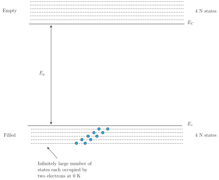
At the actual interatomic distance in Si and Ge crystal lattices, the energy band of these states splits into two bands, separated by an energy gap (Figure 14.1).
The lower band — completely occupied by the valence electrons at absolute zero temperature — is the valence band. The upper band — consisting of energy states and completely empty at absolute zero — is the conduction band.
The lowest energy level in the conduction band is denoted , and the highest energy level in the valence band is denoted . Above and below there are a large number of closely spaced energy levels.
The gap between the top of the valence band and the bottom of the conduction band is called the energy band gap (or simply energy gap), denoted . Its magnitude — large, small, or zero — determines whether a material is a metal, semiconductor, or insulator.
Three Cases: Metals, Insulators, and Semiconductors
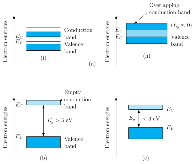
Case I — Metals (Figure 14.2a)
A metal can arise in two ways:
- The conduction band is partially filled and the valence band is partially empty.
- The conduction band and valence band overlap.
When there is overlap, electrons from the valence band can easily move into the conduction band. This makes a large number of electrons available for electrical conduction. When the valence band is partially empty, electrons from its lower levels can move to higher levels within the band, also making conduction possible. Consequently, such materials have low resistance (high conductivity). …
Drawn by us to help you understand the concept clearly, and verified to make sure it's accurate. For exams, practice from your textbook's own diagram.
What Fig. 14.1 Shows
The diagram is an energy-band diagram for a semiconductor at absolute zero temperature (0 K). Energy increases upward along the vertical axis. Two horizontal bands are drawn as tall rectangles, each filled with many closely spaced horizontal lines representing individual energy states.
The lower rectangle is the valence band, explicitly labelled "Filled" on the real figure and marked "4 N states" — at 0 K it is completely filled with electrons. A leader line inside this band points to a cluster of dots annotated "Infinitely large number of states each occupied by two electrons at 0 K." Its topmost energy level is labelled . The upper rectangle is the conduction band, explicitly labelled "Empty" and also marked "4 N states" — at 0 K it is completely empty, no electrons occupy it. Its lowest energy level is labelled .
Between these two bands lies a clear, empty region called the energy band gap or simply the energy gap, marked with a vertical double-headed arrow and labelled . This gap represents the minimum energy an electron in the valence band must gain to jump into the conduction band and become free to conduct electricity.
The figure also carries the labels "Conduction band" and "Valence band" beside their respective rectangles.
The Physical Idea
At 0 K, every electron in a pure semiconductor sits in the valence band, bound to its parent atom. No electrons are available in the conduction band, so the material behaves as a perfect insulator. The energy gap is the barrier that electrons must overcome.
The key insight is that this gap is small — typically less than 3 eV for semiconductors like silicon (1.1 eV) or germanium (0.7 eV). At room temperature, a tiny fraction of valence electrons gain enough thermal energy to cross and reach the conduction band. Once there, they can move freely under an electric field, giving the semiconductor its intermediate conductivity.
The textbook emphasises that the conduction band contains "infinitely large number of closely spaced energy states" and the valence band contains "closely spaced completely filled energy states." This means the bands are not single energy levels but continuous ranges of allowed energies.
The Central Formula
The figure directly leads to the most important formula in semiconductor physics — the temperature dependence of carrier concentration:
where:
- is the intrinsic carrier concentration (number of electrons or holes per unit volume in a pure semiconductor)
- is the effective density of states in the conduction band
- is the effective density of states in the valence band
- is the energy band gap (the vertical distance between and in the figure)
- is Boltzmann's constant ( J/K)
- is the absolute temperature in kelvin
The exponential factor tells you that even a small change in or dramatically changes the number of charge carriers. This is why silicon (with eV) and germanium ( eV) behave so differently at the same temperature.
A common mistake is to think the energy gap is the energy difference between any two arbitrary levels in the bands. It is specifically the gap between the top of the valence band () and the bottom of the conduction band () — the minimum energy an electron needs to become free.
How the Figure Connects to the Classification of Solids
The textbook uses this figure as a foundation to classify all solids into three categories: …
Drawn by us to help you understand the concept clearly, and verified to make sure it's accurate. For exams, practice from your textbook's own diagram.
What Fig. 14.2 Shows
The figure presents three vertical energy-band diagrams side by side, labelled (a), (b), and (c). Each diagram has two horizontal bands: the conduction band (upper) and the valence band (lower). The vertical direction represents increasing electron energy. The key difference between the three panels is the size of the energy gap — the forbidden region between the top of the valence band and the bottom of the conduction band.
Panel (a) — Metals: the real figure actually draws TWO distinct sub-diagrams for the metal case, side by side. Sub-diagram (a)(i) shows the conduction band () and valence band () drawn close together but still as separate bands — this depicts a metal where the conduction band is partially filled and the valence band is partially empty, so electrons are already available for conduction without crossing any gap. Sub-diagram (a)(ii) shows a genuinely overlapping case: a single merged solid block labelled "Overlapping conduction band," with and both marked close together inside it and noted explicitly. Either way — partially-filled bands or true overlap — electrons are free to move into the conduction band without needing any external energy, which is why metals have very high electrical conductivity.
Panel (b) — Insulators: A large energy gap separates the two bands, with . Following the same fill convention as Fig. 14.1, the valence band is drawn solid/filled and the conduction band is drawn hollow/light to show it is empty. Because the gap is so large, thermal energy at room temperature (about ) cannot excite electrons across it. No electrons are available in the conduction band, so the material conducts almost no electricity.
Panel (c) — Semiconductors: A small but finite energy gap exists, with . At absolute zero, the valence band is full and the conduction band is empty — the material behaves like an insulator. But at room temperature, some valence electrons gain enough thermal energy to jump across the small gap into the conduction band. These few electrons (and the holes they leave behind) make the material weakly conducting — much less than a metal, but far more than an insulator.
The energy band gap is the single most important parameter that determines whether a solid is a metal, insulator, or semiconductor. It is defined as:
where is the energy of the lowest level in the conduction band and is the energy of the highest level in the valence band.
The Physical Idea
The figure teaches a fundamental principle: electrical conduction in solids depends on whether electrons can move into the conduction band. In a metal, the bands overlap — electrons are already free. In an insulator, the gap is too large for thermal excitation to work. In a semiconductor, the gap is small enough that a tiny fraction of electrons can be thermally excited into the conduction band, giving it intermediate conductivity.
This is why semiconductors are so useful: their conductivity can be controlled by temperature, by adding impurities (doping), or by shining light on them — all of which can provide the extra energy needed to push more electrons across the gap.
A common mistake is to think that semiconductors have "some" electrons in the conduction band at all temperatures. At absolute zero (0 K), a pure semiconductor behaves exactly like an insulator — the conduction band is completely empty. It is only at higher temperatures that thermal excitation creates charge carriers.
The Key Formula
The textbook uses this figure to introduce the concept of the energy gap, but the most important formula that follows from this picture is the temperature dependence of conductivity in semiconductors:
where: …