Physics · Ch 14 — Semiconductor Electronics: Materials, Devices and Simple Circuits
Application of Junction Diode as a Rectifier
Application of Junction Diode as a Rectifier
14.7 Application of Junction Diode as a Rectifier
The Core Idea: From AC to Pulsating DC
A junction diode's V-I characteristic reveals a one-way street: current flows freely only when the diode is forward biased. When you apply an alternating voltage across a diode, current flows only during those parts of the AC cycle where the diode finds itself forward biased. This property — called rectification — is the foundation of every DC power supply.
The circuit that performs this conversion is a rectifier. Place a diode in series with a load resistor , apply an AC voltage across the combination, and you get a pulsating voltage across — but only during those half-cycles when the diode conducts. The output, though still varying, flows in one direction only. That unidirectional output is called rectified voltage.
The reverse breakdown voltage of the diode must be chosen sufficiently higher than the peak AC voltage from the transformer secondary. If the reverse voltage exceeds the breakdown rating, the diode will be destroyed.
Half-Wave Rectifier
Circuit and Working
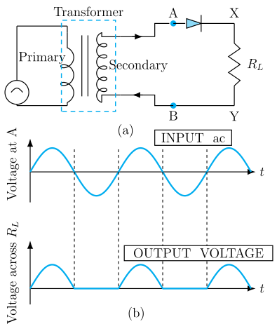
Figure 14.18(a) shows the simplest rectifier circuit. A transformer supplies the desired AC voltage across terminals A and B. The diode and load resistor are in series with this secondary winding.
Operation in the positive half-cycle: When terminal A is positive with respect to B, the diode is forward biased. It conducts, and current flows through . An output voltage appears across , following the shape of the positive half of the input sine wave.
Operation in the negative half-cycle: When A becomes negative, the diode is reverse biased. The reverse saturation current is negligible — for all practical purposes, zero. No current flows through , and the output voltage is zero.
The next positive half-cycle repeats the pattern. The output, shown in Fig. 14.18(b), consists of pulses that match the positive halves of the input AC wave. Since only half of each input cycle appears at the output, this circuit is called a half-wave rectifier.
Key Characteristics
The output is unidirectional but not steady — it is a train of half-sinusoid pulses. This pulsating DC still contains an AC component (called ripple) and needs further smoothing for most practical applications.
Full-Wave Rectifier
Why Go Full-Wave?
A half-wave rectifier wastes half the input cycle. A full-wave rectifier captures both halves, giving a more efficient conversion — more output power and less ripple for the same transformer rating.
The Centre-Tap Transformer Circuit
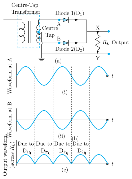
Figure 14.19(a) shows the classic full-wave rectifier using two diodes. The secondary winding of the transformer has a centre tap — a connection at the midpoint of the winding. This creates two equal voltages, and , that are out of phase with each other.
Connections:
- The p-side (anode) of diode connects to terminal A.
- The p-side of diode connects to terminal B.
- The n-sides (cathodes) of both diodes are joined together.
- The load resistor connects between this common cathode point and the centre tap.
- The output is taken across .
Working Through One Full Cycle
Positive half-cycle (A positive, B negative relative to centre tap):
- Diode is forward biased (its anode is positive with respect to its cathode, which is at centre-tap potential through ). conducts.
- Diode is reverse biased (its anode at B is negative). does not conduct.
- Current flows from A through , through (top to bottom), and back to the centre tap. Output voltage appears across .
Negative half-cycle (A negative, B positive relative to centre tap):
- Diode is now reverse biased. It does not conduct.
- Diode is forward biased. conducts.
- Current flows from B through , through (still top to bottom — same direction!), and back to the centre tap.
Notice the critical detail: current through flows in the same direction during both halves of the AC cycle. This is what gives full-wave rectification — both halves contribute to the output.
The output waveform, shown in Fig. 14.19(c), consists of half-sinusoid pulses occurring twice per input cycle — one from each diode. The frequency of the output pulses is double the input AC frequency.
The Four-Diode Alternative (Bridge Rectifier)
The textbook notes that another full-wave rectifier circuit exists that does not need a centre-tap transformer but requires four diodes. This is the bridge rectifier — it uses the full secondary voltage and is more common in practice because centre-tap transformers are bulkier and more expensive.
Filtering: From Pulsating to Steady DC
The rectified output, whether half-wave or full-wave, is a series of pulses. It is unidirectional but not constant — it rises and falls with each pulse. Most electronic circuits need a steady DC voltage. The solution is a filter.
The Capacitor Filter
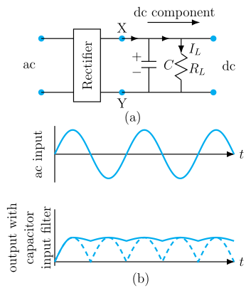
The simplest and most widely used filter is a capacitor connected in parallel with the load resistor (Fig. 14.20(a)). An inductor in series with can also serve as a filter, but the capacitor filter is the standard choice.
How it works:
-
Charging phase: When the rectified voltage rises (during a pulse), the capacitor charges up. If there were no load, it would charge to the peak voltage and stay there.
-
Discharging phase: When the rectified voltage falls (between pulses), the capacitor discharges through the load resistor . The voltage across the capacitor (and hence across ) does not drop to zero — it falls gradually.
-
Recharging: When the next pulse arrives, the capacitor recharges back to the peak voltage. …
Drawn by us to help you understand the concept clearly, and verified to make sure it's accurate. For exams, practice from your NCERT textbook's own diagram.
Figure 14.18 is the first rectifier circuit a student meets, and it teaches a simple but profound idea: a single diode can convert an alternating voltage into a unidirectional (but still pulsating) voltage. The figure has two panels, (a) and (b), and you must read them together.
Panel (a) shows the circuit. A transformer steps the mains ac voltage up or down as needed; its secondary winding has two terminals labelled A and B. Terminal A is connected to the anode of a single diode. The cathode of that diode connects to one end of a load resistor . The other end of returns to terminal B, completing the loop. That is the entire circuit — one diode, one resistor, and a transformer. There is no centre tap, no second diode, no capacitor.
Panel (b) shows two waveforms stacked vertically, both plotted against time on the horizontal axis. The upper waveform is the input ac voltage across the secondary (between A and B). It is a pure sinusoid: it rises smoothly from zero to a positive peak, falls back through zero, goes to a negative peak of equal magnitude, and returns to zero — one full cycle. The lower waveform is the output voltage measured across . Here the negative half-cycles are completely absent; the output is zero during those intervals. Only the positive half-cycles appear, each shaped like the top half of a sine wave — a series of humps separated by flat zero segments. The output is therefore a train of positive pulses, one per input cycle.
The output is called rectified because it flows in only one direction through , but it is not steady dc — it still varies from zero to a peak value. That is why the textbook later adds a capacitor filter to smooth it out.
The physical idea is straightforward. A diode conducts only when forward biased (anode positive with respect to cathode). During the positive half-cycle of the input, terminal A is positive relative to B, so the diode is forward biased and current flows through , producing a voltage drop across it. During the negative half-cycle, A is negative relative to B, the diode is reverse biased, and the reverse saturation current is so small (essentially zero for practical purposes) that no appreciable current flows. Hence the output voltage is zero. The diode must be chosen so that its reverse breakdown voltage exceeds the peak input voltage; otherwise it would be destroyed during the reverse-biased half-cycles. …
Drawn by us to help you understand the concept clearly, and verified to make sure it's accurate. For exams, practice from your NCERT textbook's own diagram.
Fig. 14.19 is the centre-piece of the full-wave rectifier discussion. It packs three panels into one figure, and each panel teaches a different part of the story: the circuit topology, the two out-of-phase inputs, and the resulting output.
Panel (a) shows the circuit. A centre-tapped transformer secondary gives two equal voltages, one from the centre tap to terminal A and one from the centre tap to terminal B. Two diodes, D1 and D2, have their p-sides connected to A and B respectively. Their n-sides are joined together at a common node. The load resistor is connected between that common node and the centre tap. This is the defining feature of a centre-tap full-wave rectifier: the load sees the voltage from the common cathode point to the centre tap, so each diode conducts on alternate half-cycles and the current through always flows in the same direction.
Panel (b) shows two input voltage waveforms, one at A and one at B, plotted against time. The key point is that they are out of phase. When A is positive with respect to the centre tap, B is equally negative, and vice versa. This phase relationship is what allows the two diodes to take turns conducting.
Panel (c) shows the output voltage across . It is a train of positive half-sinusoid humps, one for every half-cycle of the input — there is no gap. During the half-cycle when A is positive, D1 conducts and the output follows the positive half of the A waveform. During the next half-cycle, B is positive, D2 conducts, and the output follows the positive half of the B waveform. The result is a full-wave rectified voltage: unidirectional but still pulsating, with a frequency twice that of the input.
The output frequency of a full-wave rectifier is double the input frequency. If the mains supply is 50 Hz, the output pulses occur at 100 Hz. This makes filtering easier than in a half-wave rectifier.
Because both halves of the ac cycle now contribute a pulse to the output, a full-wave rectifier delivers a steadier, more efficient output than a half-wave rectifier for the same transformer — the output pulses are twice as frequent and the gaps between them are gone. The output in panel (c) is still not steady dc, though; like the half-wave case, it still has significant ripple, which is why the textbook follows this figure with a discussion of the capacitor filter (Fig. 14.20) to smooth it into something close to steady dc. …
Drawn by us to help you understand the concept clearly, and verified to make sure it's accurate. For exams, practice from your NCERT textbook's own diagram.
Fig. 14.20 is the textbook’s way of showing you how a simple capacitor turns the bumpy, pulsating output of a full-wave rectifier into a much smoother, nearly steady dc voltage. The figure has two panels, (a) and (b), and you need to understand both to see the full story.
Panel (a) is the circuit diagram. It is exactly the full-wave rectifier from Fig. 14.19 — two diodes and , a centre-tapped transformer, and a load resistor — but now with one extra component: a capacitor connected in parallel across . This capacitor is the filter. It sits directly across the output terminals, so the same voltage that appears across also appears across . The textbook calls this a capacitor-input filter because the rectified voltage first “sees” the capacitor before the load.
Panel (b) is actually TWO separate stacked panels sharing the same time axis, not a single plot -- confirmed against the real page. The TOP panel, labelled “ac input,” simply re-draws the original ac source waveform: a plain, undistorted sine wave, swinging equally positive and negative, identical in shape to the input waveform in Figs 14.18 and 14.19. It is not a rectifier output at all -- it is shown so you can compare the filtered output's ripple rate against the original ac cycle. The BOTTOM panel, labelled “output with capacitor input filter,” is where the capacitor's effect is actually shown, and it is this panel -- not the whole of (b) -- that carries two curves on one set of axes. The dashed curve shows the output of the full-wave rectifier without the filter — the familiar train of half-sinusoid humps, one for each half-cycle of the ac input, touching zero between humps. This is the pulsating dc that the rectifier alone produces. The solid curve shows the voltage across the capacitor (and therefore across ) with the filter in place. This solid line is the smoothed output: it rises quickly with the first hump, charging the capacitor to nearly the peak voltage, and then, as each rectified hump falls back toward zero, the capacitor discharges slowly through instead of following it down, producing a shallow downward droop; the next hump recharges the capacitor back to the peak before it can droop far, and the cycle repeats. The result is a voltage that stays close to the peak value throughout, with only a small periodic variation called the ripple -- the shallow sawtooth-like dips on the solid curve, spaced at twice the input frequency (once per rectified hump).
The physical idea is straightforward: the capacitor stores charge when the rectified voltage is high, and releases that charge to the load when the rectified voltage drops. This “fills in the gaps” between the humps. Without the capacitor, the output falls to zero between humps; with the capacitor, it never falls that low. The quality of the smoothing depends on how slowly the capacitor discharges, which is governed by the time constant .
The key result the textbook develops with this figure is the condition for good smoothing: the time constant must be much larger than the time between successive charging peaks. For a full-wave rectifier operating at mains frequency , the charging peaks occur every seconds. So the requirement is
When this holds, the capacitor discharges only a little between peaks, and the ripple voltage is small.
The ripple voltage itself can be estimated. If the capacitor discharges approximately linearly (a good approximation when the ripple is small), the charge lost during one discharge interval is , where is the average load current. The corresponding voltage drop (the ripple) is
This formula is not given explicitly in the textbook text you provided, but it follows directly from the physics of capacitor discharge and is the standard result for a full-wave rectifier with a capacitor filter. A larger or a smaller load current (larger ) gives a smaller ripple — a smoother dc output. …