Q.Draw circuit diagram for a P-N junction to obtain reverse bias characteristic curves. Explain the phenomenon of reverse breakdown for a P-N junction in reverse bias state by following processes- i) Avalanche breakdown ii) Zener breakdown [1 + 2 = 3]
You're viewing a preview — the full solution, concept, methods & PYQ mapping are locked.
Start your 14-day free trial to unlock the full solution →Reverse-biased p-n junction passes tiny leakage current until breakdown; avalanche = impact-ionisation chain, Zener = direct field breaking of bonds.
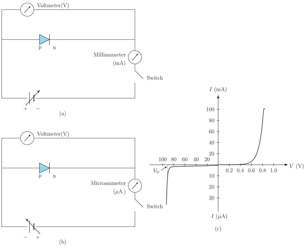
Circuit diagram (describe/draw): Connect the p-side of the junction diode to the negative terminal and the n-side to the positive terminal of a variable DC supply (reverse bias). Place a microammeter (μA) in series to read the small reverse current and a voltmeter across the diode to read the reverse voltage. Vary the reverse voltage and plot reverse current (μA, on the negative y-axis) against reverse voltage (negative x-axis): the current stays very small and nearly constant (reverse saturation current) until the breakdown voltage, beyond which the reverse current increases very sharply.
Reverse breakdown mechanisms:
i) Avalanche breakdown: This occurs in lightly-doped junctions (wide depletion region) at high reverse voltages. The minority carriers are accelerated by the strong field and gain large kinetic energy. On colliding with atoms of the crystal lattice, they knock out valence electrons (impact ionisation), creating new electron–hole pairs. These new carriers are again accelerated and produce still more pairs — a cumulative (avalanche) multiplication of carriers — so the reverse current rises abruptly.
…
Unlock everything free for 14 days
- Full step-by-step solutions
- Concept-first explanations
- Methods, shortcuts & mistakes
- PYQ mapping + timed mock tests
Full access for 14 days. No credit card required.