Physics · Ch 14 — Semiconductor Electronics: Materials, Devices and Simple Circuits
Semiconductor Diode
Semiconductor Diode
The Semiconductor Diode
A semiconductor diode is simply a p-n junction equipped with metallic contacts on both ends, allowing an external voltage to be applied across it. It is a two-terminal device — one terminal connected to the p-side, the other to the n-side.
The circuit symbol for a p-n junction diode is shown in Fig. 14.12(b). The arrow in the symbol points in the conventional direction of current flow when the diode is forward-biased (i.e., when the p-side is at a higher potential than the n-side). The flat bar at the arrow's tail represents the n-side, and the arrowhead represents the p-side.
The arrow direction is crucial: it always points from the p-region to the n-region under forward bias, matching the conventional current direction (positive charge flow).
The Barrier Potential Under Bias
In equilibrium (no external voltage), a built-in potential barrier exists across the depletion region of the p-n junction (Fig. 14.11). This barrier prevents further diffusion of majority carriers across the junction.
When an external voltage is applied across the diode, this equilibrium barrier potential is altered. The applied voltage either reduces or increases the barrier height, depending on its polarity — this is the fundamental principle behind diode operation: by controlling the barrier height with an external voltage, we can either allow current to flow easily or block it almost entirely.
Forward Bias and Reverse Bias
The two possible ways to connect an external voltage to a diode are:
Forward bias: The p-side is connected to the positive terminal of the battery, and the n-side to the negative terminal. The applied voltage opposes the built-in potential, reducing the barrier height to (Fig. 14.13). Majority carriers (holes from p-side, electrons from n-side) can now cross the junction more easily, resulting in a significant current — typically in the milliampere range.
Reverse bias: The p-side is connected to the negative terminal, and the n-side to the positive terminal. The applied voltage adds to the built-in potential, increasing the barrier height to (Fig. 14.15). Majority carriers are pushed away from the junction, widening the depletion region. Only a very small reverse saturation current flows, carried by minority carriers — typically a few microamperes.
A common mistake is to think that forward bias means "current flows easily" in both directions. The diode only conducts significantly in one direction — forward bias. In reverse bias, the current is negligible (microamperes or less) until breakdown occurs.
Cut-in (Threshold) Voltage
For forward bias, the current remains very small until the applied voltage crosses a certain threshold, called the cut-in voltage or threshold voltage. Beyond this voltage, the current increases significantly. For silicon diodes this threshold is about V; for germanium diodes it is about V.
The cut-in voltage is not a fundamental constant of the p-n junction — it is a practical observation of the applied voltage at which conduction becomes significant. It depends on the diode material and, to a lesser extent, on temperature and doping.
Dynamic Resistance
For diodes, a useful quantity is the dynamic resistance — the ratio of a small change in voltage to the corresponding small change in current:
…
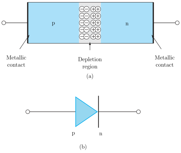
Drawn by us to help you understand the concept clearly, and verified to make sure it's accurate. For exams, practice from your textbook's own diagram.
Figure 14.12 is the textbook's first look at a real semiconductor diode — it bridges the abstract p-n junction studied in earlier diagrams (like Fig. 14.11) with the practical two-terminal device used in circuits.
Panel (a) shows the physical construction: a bar of semiconductor material divided into a p-region and an n-region. Metallic contacts are attached at both ends — these are the leads that let you apply an external voltage. Without those contacts, you cannot connect the junction to a battery or a circuit. The labels "p" and "n" mark the two sides of the junction itself, and "Depletion region" labels the junction area.
Panel (b) gives the standard circuit symbol. A solid triangle points toward a short perpendicular bar. The triangle represents the p-side (the anode), and the bar represents the n-side (the cathode). The arrowhead of the triangle points in the direction of conventional current when the diode is forward biased — that is, when the p-side is made positive relative to the n-side. This is a crucial visual cue: the symbol itself tells you which way current is allowed to flow easily.
The arrow in the diode symbol always points from the p-side (anode) to the n-side (cathode) — the direction of forward current. Current cannot flow in the opposite direction under normal forward bias conditions.
The physical point this figure sets up: the equilibrium barrier potential (the built-in voltage that exists across the depletion region when no external voltage is applied) can be altered by applying an external voltage across the diode. Forward bias reduces the effective barrier to , allowing majority carriers to cross the junction and produce a significant current; reverse bias increases the barrier to , suppressing current flow almost entirely. …