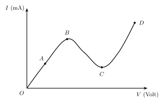
Q.In the given diagram, identify the region that has negative resistance.
🔒You're viewing a preview — the full solution, concept, methods & PYQ mapping are locked.
🔒 Start your 14-day free trial to unlock the full solution →Concept understanding — p-n Junction Diode
When p-type and n-type semiconductor material are joined, the result is a p-n junction -- the structural basis of almost every modern semiconductor device. Immediately after joining, a large density gradient of each carrier type exists across the junction, driving DIFFUSION: electrons migrate from the electron-rich n-side into the p-side, and holes migrate from the hole-rich p-side into the n-side. This leaves behind FIXED, immobile ions near the junction -- positively charged donor ions on the n-side (where electrons departed) and negatively charged acceptor ions on the p-side (where holes departed). Because free carriers cannot survive within a region containing this exposed ionic charge, the region straddling the junction becomes essentially empty of mobile carriers -- the DEPLETION REGION -- and the accumulated ionic charge on both sides sets up a permanent POTENTIAL BARRIER (about 0.6-0.7 V for silicon, 0.3-0.35 V for germanium) that exists even with no external voltage connected, bringing the junction to electrostatic equilibrium with an internal field pointing from the n-side toward the p-side. …
Resistance is normally positive because current rises as voltage rises, so a negative-resistance region is one where the current actually falls while the voltage keeps increasing. On this characteristic that behaviour occurs only along the descending stretch between the peak and the valley. …
Negative resistance means current DEcreases as voltage increases -- that only happens on the segment between the peak (B) and the valley (C) of this tunnel-diode-like I-V curve.
Resistance, expressed as the slope dV/dI, is normally positive because current increases as voltage increases. In this characteristic curve, current rises from O through A to a peak at B, then over the segment B to C, current actually DEcreases even though voltage keeps increasing (before rising again from C to D). Over that B-to-C stretch, dVdI<0, i. …
- CBSE 2025Set ANNUAL1 markQ.Draw a labelled experimental circuit arrangement for studying the V-I characteristic curves of a p-n junction diode in forward bias.
›Reveal solutionSolution
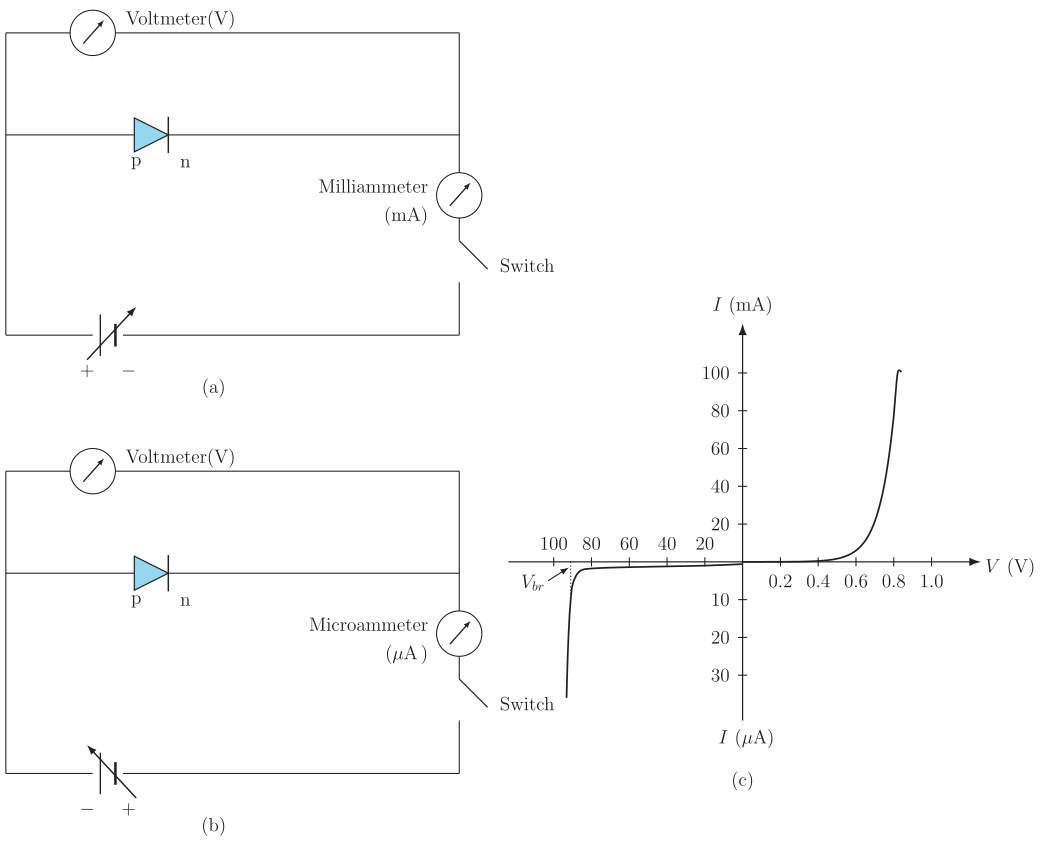
Figure — Stem asks for the labelled experimental circuit to study the forward-bias V-I characteristic of a p-n diode; t To trace the forward V-I characteristic, the diode is forward-biased through a variable-voltage source and a current-limiting resistor, with a voltmeter across the diode and a milliammeter in series to record corresponding V and I readings.
A labelled circuit description (since this is a diagram question, the arrangement is described precisely below):
- A p-n junction diode is connected in forward bias: its p-side (anode) connected through a rheostat (variable resistor, to limit/control current) to the positive terminal of a DC battery, and its n-side (cathode) connected to the battery's negative terminal, completing the loop.
- A milliammeter (mA) is connected in series in this loop, to measure the forward current If through the diode.
- A voltmeter (V) is connected in parallel directly across the diode terminals, to measure the forward voltage Vf across it.
- A key/switch is included in series to open/close the circuit. …
- CBSE 2024Set FS1 markQ.How much charge is there on hole? Draw the circuit symbol of p-n junction diode.
›Reveal solutionSolution
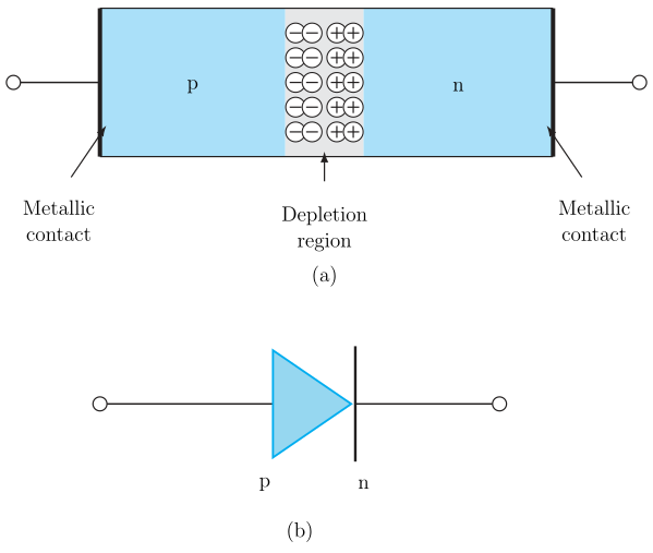
Figure — The stem's explicit 'Draw the circuit symbol of p-n junction diode' is a hard draw gate; the catalog carries t A hole carries a positive charge +e=+1.6×10⁻¹⁹ C; the diode symbol is an arrowhead (p, anode) pointing to a bar (n, cathode).
Charge on a hole. A hole is the vacancy left when a covalent bond loses an electron. It behaves exactly like a free particle carrying a positive charge equal in magnitude to the electron's, i.e.
qhole=+e=+1.6×10⁻¹⁹ C.
…
- CBSE 2024Set ANNUAL1 markMCQQ.PN Junction diode is :(a) ohmic resistance(b) non-ohmic resistance(c) negative resistance(d) positive resistance
›Reveal solutionSolution
The diode's V–I curve is not a straight line through the origin, so it does not obey Ohm's law.
Ohm's law, V=IR with constant R, holds only for conductors whose V–I graph is a straight line through the origin (ohmic devices, e.g. a metal wire at constant temperature). A PN junction diode's V–I characteristic is strongly non-linear: negligible current flows until the forward voltage crosses the barrier potential (~0.6–0.7 V for silicon), after which current rises st …
- CBSE 2023Set F1 markMCQQ.→| is the symbol of (A) diode (B) n-type (C) p-type (D) transistor
›Reveal solutionSolution
The arrow-into-bar symbol is the circuit symbol of a p-n junction diode.
In the standard circuit symbol of a semiconductor diode, the triangle (arrow) represents the p-side (anode) and the bar represents the n-side (cathode). The arrow points in the direction …
- CBSE 2020Set NC1 markQ.What is V-I characteristic of a p-n junction diode? Draw the V-I characteristic of a diode in forward bias.
›Reveal solutionSolution
A diode's V-I characteristic shows how strongly it conducts as a function of the voltage across it — in forward bias, it stays almost off until the barrier potential is overcome, then conducts very freely.
Definition
The V-I (voltage-current) characteristic of a diode is a plot of the current I flowing through it against the voltage V applied across it, showing how the diode's conduction depends on bias.
Forward-bias characteristic (diagram description)
…
- CBSE 2016Set ANNUAL1 markMCQQ.What will happen if the amount of reverse biasing in a p-n junction diode is gradually increased?(a) Thickness of depletion region will increase(b) Flow of current due to majority carriers will increase(c) Thickness of depletion region will decrease(d) Flow of current due to majority carriers will decrease
›Reveal solutionSolution
Reverse bias pulls majority carriers further away from the junction, widening the depletion region and drastically reducing current.
In reverse bias, the applied voltage attracts the majority carriers (electrons in the n-side, holes in the p-side) away from the junction, widening the depletion region and increasing the potential barrier. This makes it harder for majority carriers to cross, so majority-carrier current becomes negligibl …
🎓Unlock everything free for 14 days
- ✓Full step-by-step solutions
- ✓Concept-first explanations
- ✓Methods, shortcuts & mistakes
- ✓PYQ mapping + timed mock tests
Full access for 14 days. No credit card required.