Q.Draw the experimental circuit for the forward and reverse bias condition of a p-n junction diode, and also plot the V-I characteristic curves for both the forward bias and reverse bias.
You're viewing a preview — the full solution, concept, methods & PYQ mapping are locked.
Start your 14-day free trial to unlock the full solution →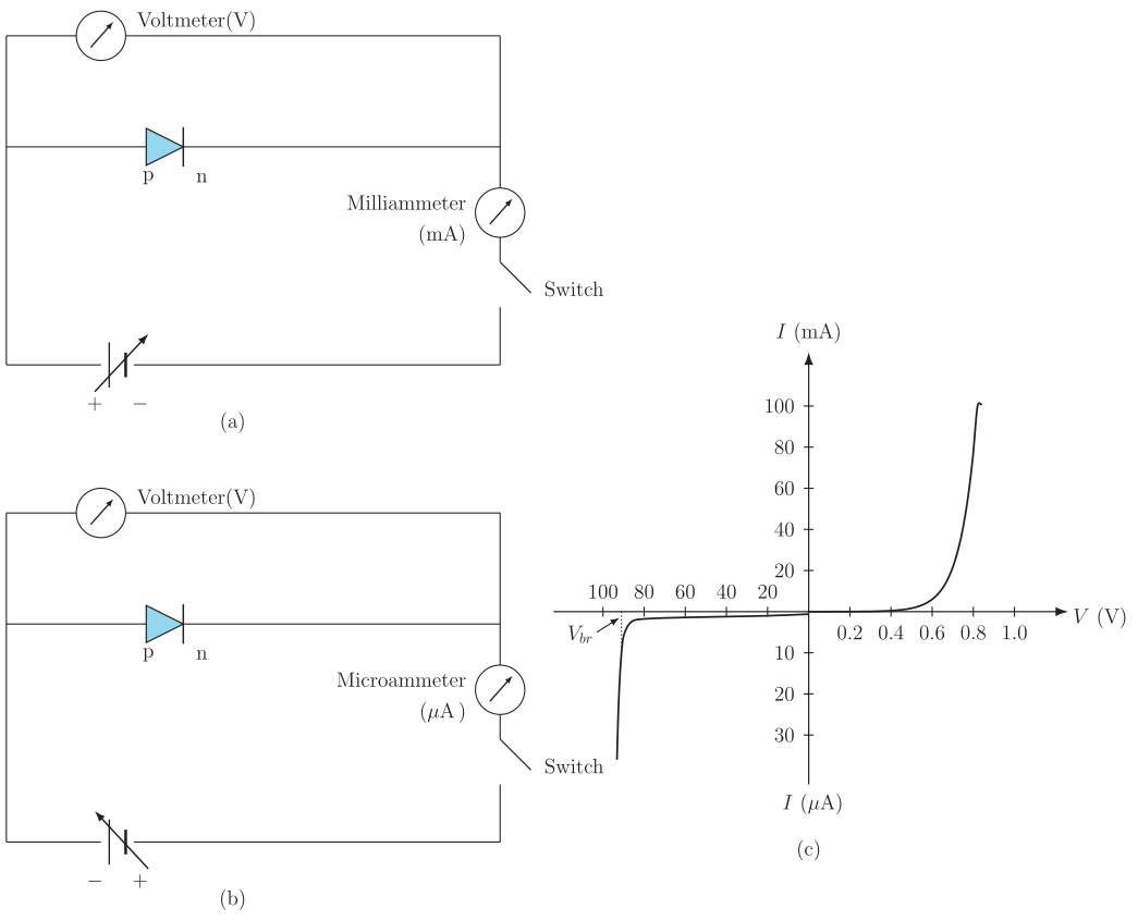
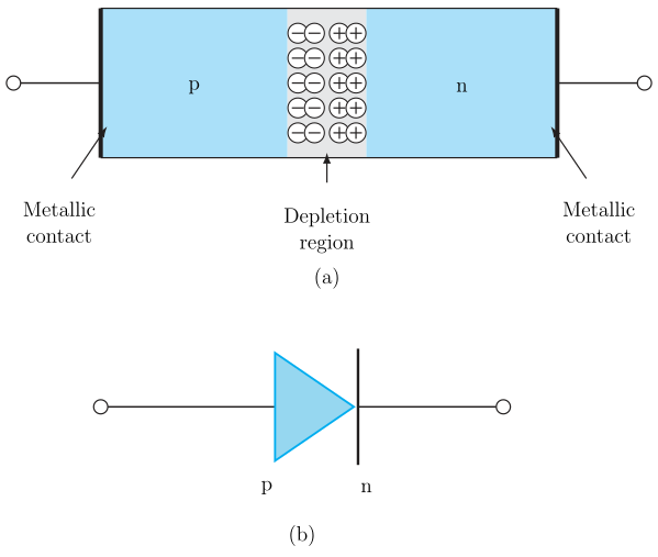
Forward bias connects the p-side to the positive terminal (low resistance, exponentially rising current above a threshold); reverse bias connects the p-side to the negative terminal (high resistance, tiny nearly-constant current).
Forward bias circuit: The p-side of the diode is connected to the positive terminal of a battery (through a rheostat/variable resistor to control voltage) and the n-side to the negative terminal, with a milliammeter connected in series (to measure the forward current ) and a voltmeter connected across the diode (to measure the forward voltage ). As the applied forward voltage is increased from 0, the current initially rises very slowly, and only after a threshold (knee) voltage (~0.3 V for Ge, ~0.7 V for Si) does the current rise sharply and almost exponentially with further small increases in voltage.
Reverse bias circuit: The p-side of the diode is connected to the negative terminal of the battery and the n-side to the positive terminal, with a microammeter in series (to measure the very small reverse current , in µA) and a voltmeter across the diode (to measure reverse voltage ). As the reverse voltage is increased, only a very small, almost constant reverse saturation current flows (due to minority carriers), until the reverse breakdown voltage is reached, beyond which the current increases suddenly and sharply (avalanche/Zener breakdown).
…
Unlock everything free for 14 days
- Full step-by-step solutions
- Concept-first explanations
- Methods, shortcuts & mistakes
- PYQ mapping + timed mock tests
Full access for 14 days. No credit card required.