Physics · Ch 14 — Semiconductor Electronics: Materials, Devices and Simple Circuits
Intrinsic Semiconductor
Intrinsic Semiconductor
Intrinsic Semiconductors: The Foundation
A pure semiconductor, with no deliberate impurities added, is called an intrinsic semiconductor. The most common examples are silicon (Si) and germanium (Ge). At absolute zero temperature ( K), an intrinsic semiconductor behaves exactly like an insulator — no electrons are available for conduction. The key difference from an insulator is that the energy gap () is small enough that at room temperature, thermal energy can promote some electrons from the valence band to the conduction band.
Crystal Structure and Covalent Bonding
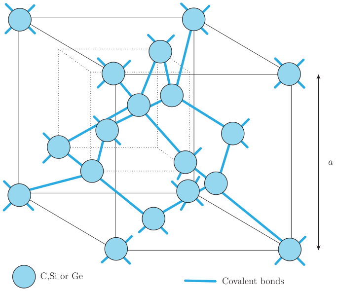
Silicon and germanium crystallise in a diamond-like structure (shown in Fig. 14.3 of the textbook). In this three-dimensional lattice, each atom is surrounded by four nearest neighbours. The lattice spacing is 5.43 Å for Si and 5.66 Å for Ge.
Both Si and Ge have four valence electrons. In the crystal, each atom shares one of its four valence electrons with each of its four neighbours, and in return receives a shared electron from each neighbour. These shared electron pairs form covalent bonds (also called valence bonds). The two shared electrons shuttle back and forth between the two atoms, holding them together strongly.
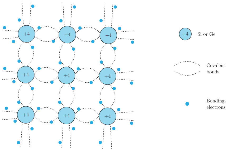
Figure 14.4 shows a simplified two-dimensional representation of this structure. At low temperatures, all covalent bonds are intact — no bonds are broken. This is an idealised picture.
The +4 symbol in Fig. 14.4 represents the inner core of the Si or Ge atom (the nucleus plus the inner electron shells). Only the four valence electrons participate in bonding.
Generation of Charge Carriers: Electrons and Holes
As temperature increases, thermal energy becomes available to the valence electrons. Some electrons gain enough energy to break away from their covalent bonds. When an electron breaks free, it becomes a free electron (charge ) that can move through the crystal and contribute to electrical conduction.
The site from which the electron escaped now has a missing electron — a vacancy in the covalent bond. This vacancy behaves as if it carries an effective positive charge . This apparent positive charge carrier is called a hole.
A hole is not a real particle. It is a convenient way to describe the absence of an electron in a covalent bond. The hole behaves as an apparent free particle with effective positive charge.
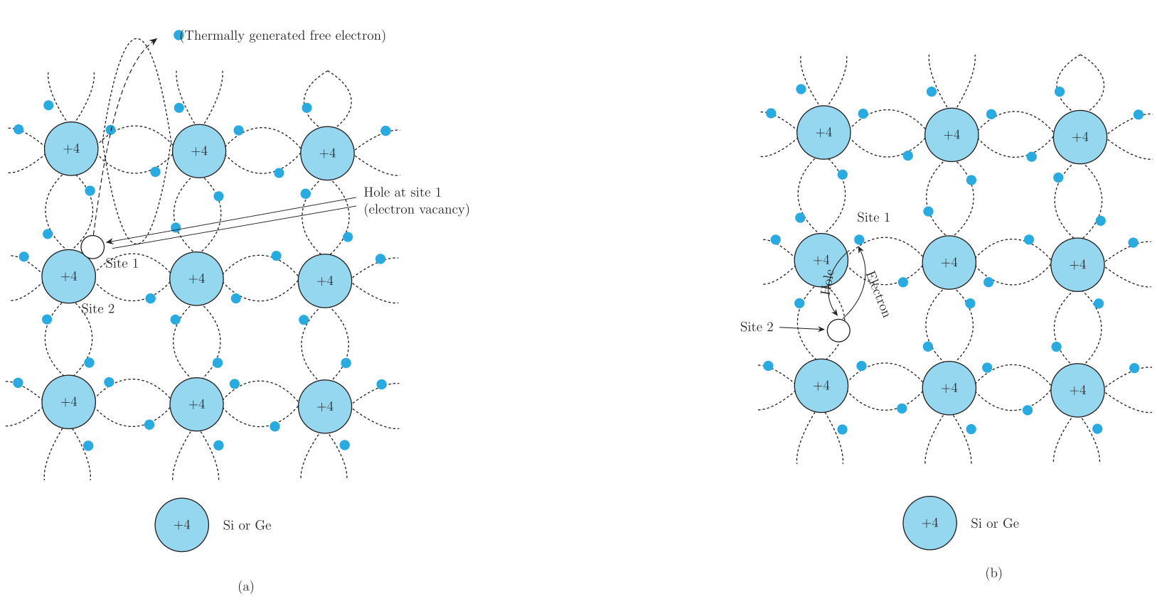
Figure 14.5(a) shows this generation process schematically. The thermal energy effectively ionises only a few atoms in the lattice, creating one free electron and one hole for each broken bond.
Intrinsic Carrier Concentration
In an intrinsic semiconductor, every broken bond creates exactly one free electron and one hole. Therefore, the number of free electrons per unit volume, , equals the number of holes per unit volume, .
Here is called the intrinsic carrier concentration. It depends on the material and temperature.
Motion of Holes: A Key Insight
Semiconductors have a unique property: apart from electrons, holes also move and contribute to current. The motion of holes is not the motion of a real particle — it is the motion of bound electrons jumping between neighbouring covalent bonds.
Consider a hole at site 1, as shown in Fig. 14.5(a). An electron from a neighbouring covalent bond at site 2 can jump into the vacant site 1. After this jump:
- Site 1 now has an electron (the hole is filled)
- Site 2 now has a vacancy (a new hole)
The hole has apparently moved from site 1 to site 2. This is shown in Fig. 14.5(b).
The free electron that was originally set free [Fig. 14.5(a)] is NOT involved in this hole motion process. The free electron moves completely independently as a conduction electron.
Current in an Intrinsic Semiconductor
When an electric field is applied:
- Free electrons move towards the positive potential, giving rise to an electron current,
- Holes move towards the negative potential, giving rise to a hole current,
The total current is the sum of both contributions:
Generation and Recombination
Two simultaneous processes occur in an intrinsic semiconductor:
- Generation: Thermal energy breaks covalent bonds, creating electron-hole pairs
- Recombination: Free electrons collide with holes and recombine, annihilating both carriers
At equilibrium, the rate of generation equals the rate of recombination. This dynamic balance maintains a constant carrier concentration at a given temperature.
Behaviour at Different Temperatures
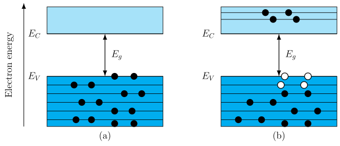
At K, an intrinsic semiconductor behaves as an insulator — the valence band is completely full and the conduction band is completely empty, as shown in Fig. 14.6(a).
At K, thermal energy excites some electrons from the valence band to the conduction band. These thermally excited electrons partially occupy the conduction band, leaving an equal number of holes in the valence band. The energy-band diagram at K is shown in Fig. 14.6(b).
Why Carbon is an Insulator While Si and Ge are Semiconductors …
Drawn by us to help you understand the concept clearly, and verified to make sure it's accurate. For exams, practice from your NCERT textbook's own diagram.
Fig. 14.3 is a three-dimensional ball-and-stick model of the diamond-cubic crystal structure — the arrangement of atoms in carbon (diamond), silicon, and germanium. The figure shows a cube with atoms placed at every corner, at the centre of each face, and at four interior positions that sit in a tetrahedral pattern. Each atom is connected by a stick (representing a covalent bond) to its four nearest neighbours, giving the entire lattice its characteristic tetrahedral bonding. A faint cube outline frames the structure, and along one edge a dimension arrow marks the lattice constant — the side length of the cube. The caption notes that for carbon , for silicon , and for germanium .
The physical idea this figure teaches is that each atom in the crystal is surrounded by exactly four nearest neighbours, and each atom shares one of its four valence electrons with each neighbour. These shared electron pairs form covalent bonds that hold the crystal together. At low temperatures, all bonds are intact and no free charge carriers exist — the material behaves like an insulator. As temperature rises, thermal energy can break some covalent bonds, freeing an electron and leaving behind a vacancy called a hole. The free electron and the hole both contribute to electrical conduction.
The textbook uses this figure to introduce the concept of intrinsic carrier concentration. In an intrinsic semiconductor, the number of free electrons equals the number of holes , and this common value is denoted :
Here is the intrinsic carrier concentration — the density of electron-hole pairs thermally generated in a pure semiconductor at a given temperature. The total current in such a material is the sum of the electron current and the hole current :
…
Drawn by us to help you understand the concept clearly, and verified to make sure it's accurate. For exams, practice from your NCERT textbook's own diagram.
What Fig. 14.4 Shows
The figure is a simplified two-dimensional sketch of the actual three-dimensional diamond-like crystal structure of silicon or germanium. Each atom is drawn as a circle labelled +4, which represents the inner core of the atom — the nucleus plus the ten tightly bound inner electrons (for Si, the configuration; for Ge, the core). The +4 charge indicates that after the four valence electrons are shared, the core effectively has a net charge of .
The atoms are arranged in a regular square grid. Every atom is connected to its four nearest neighbours (up, down, left, right) by a covalent bond, drawn on the real figure as a dashed/scalloped curved line with small dots placed along it — the dashed line represents the bond itself and each dot represents one of the two shared bonding electrons (the figure's own legend lists these as two separate symbols: the bond line, and the bonding electron dot). This is the textbook's "overemphasised" two-dimensional picture: in reality, the bonds are not all in one plane, but the essential idea of four bonds per atom is correct.
The key point of the figure is that every bond is intact. No bonds are broken, no electrons have been knocked loose. This is the situation at very low temperatures (near 0 K), where thermal energy is insufficient to break any covalent bonds. The crystal is a perfect insulator at this stage — there are no free charge carriers.
The Physical Idea
The figure establishes the reference state for understanding how semiconductors conduct. In this idealised low-temperature picture, all four valence electrons of each Si or Ge atom are locked into covalent bonds. These electrons are not free to move through the crystal; they are localised between pairs of atoms. Consequently, there are no conduction electrons and no holes — the material behaves like an insulator.
As temperature rises, thermal energy becomes available. Some electrons gain enough energy to break free from their covalent bonds. When an electron leaves a bond, it becomes a free electron (charge ) that can move through the crystal and contribute to conduction. The vacancy it leaves behind — a missing electron in what was a complete bond — behaves as a hole with an effective positive charge . This is shown in the subsequent Fig. 14.5(a), which builds directly on the intact-bond picture of Fig. 14.4.
The hole is not a real particle. It is a convenient way to describe the collective motion of bound electrons. When a neighbouring electron jumps into the hole, the hole appears to move in the opposite direction. This apparent motion of positive charge contributes to current just as real positive charges would.
The Key Formula
The textbook uses this figure to introduce the fundamental relation for intrinsic semiconductors:
Here:
- is the number density of free electrons (conduction electrons) per unit volume
- is the number density of holes per unit volume
- is the intrinsic carrier concentration — the common value for a pure, undoped semiconductor at a given temperature
The equality follows directly from the generation process shown in Fig. 14.5(a): every time a covalent bond breaks, it creates exactly one free electron and one hole. No other source of charge carriers exists in an intrinsic semiconductor. The total current is the sum of electron and hole contributions:
where is the electron current and is the hole current.
Do not confuse the +4 label on each atom with the charge on a hole. The +4 is the net charge of the atomic core (nucleus plus inner electrons). A hole has an effective charge of (where C), which is much smaller and arises from the absence of a valence electron, not from the core itself.
Why This Matters for the Energy Band Picture …
Drawn by us to help you understand the concept clearly, and verified to make sure it's accurate. For exams, practice from your NCERT textbook's own diagram.
Fig. 14.5 is the key picture that makes the idea of a “hole” physically concrete. It shows two snapshots of the same small piece of a silicon or germanium crystal, drawn as a 2‑D grid of +4 cores connected by covalent bonds (each bond is a pair of shared electrons).
Panel (a) shows what happens when thermal energy breaks one covalent bond. At the site labelled site 1, the bond is missing one electron — that electron has been knocked free and is now a conduction electron, shown as a separate particle moving away from the lattice with the text label "(Thermally generated free electron)." The empty bond position left behind is the hole, marked with the text label "Hole at site 1 (electron vacancy)." (Note: the real figure labels these two events with plain text only — it does not print ""/"" charge symbols directly on the diagram; the charge notation is discussed only in the surrounding body text.) So in (a) you see the generation of an electron–hole pair: one free electron and one hole, created together.
Panel (b) shows how the hole can appear to move. An electron from a neighbouring intact bond at site 2 (lower‑left in the figure) jumps along an arrow into the hole at site 1. After that jump, site 1 now has a complete bond (the hole is filled), but site 2 now has a missing electron — a new hole. The hole has apparently shifted from site 1 to site 2. The original free electron from panel (a) is not involved in this motion; it moves independently through the crystal.
The hole is not a real particle. It is a convenient way to describe the collective motion of many bound electrons. When one bound electron fills a hole, it leaves a hole behind, so the vacancy propagates like a positive charge moving in the opposite direction.
The physical idea is that in an intrinsic semiconductor at moderate temperatures, thermal energy creates a small number of electron–hole pairs. Both the free electrons and the holes can carry current. The textbook uses this figure to introduce the intrinsic carrier concentration:
where is the number density of free electrons, is the number density of holes, and is the intrinsic carrier concentration (a material‑ and temperature‑dependent constant). Because each broken bond creates one electron and one hole, the two densities are equal in a pure (intrinsic) semiconductor.
The total current under an applied electric field is the sum of the electron current and the hole current:
Here is due to the drift of free electrons (negative charges moving toward the positive terminal), and is due to the apparent drift of holes (positive‑effective charges moving toward the negative terminal). The figure makes clear that these two contributions come from the same fundamental process — bond breaking — but the carriers move independently once created. …
Drawn by us to help you understand the concept clearly, and verified to make sure it's accurate. For exams, practice from your NCERT textbook's own diagram.
Fig. 14.6 is an energy-band diagram, not a plot with axes. It shows two vertical panels side by side, labelled (a) and (b). In each panel, you see two horizontal bands: the upper one is the conduction band and the lower one is the valence band. The vertical gap between them is the forbidden energy gap . The left panel, (a), is labelled “ K”. Here the conduction band is completely empty — no electrons — and the valence band is completely filled. The right panel, (b), is labelled “ K”. In this panel, four filled circles (electrons) appear in the conduction band, and four empty circles (holes) appear in the valence band. The labels and mark the bottom of the conduction band and the top of the valence band, respectively.
The physical idea is straightforward. At absolute zero, every electron sits in the lowest possible energy state. In an intrinsic semiconductor, that means the valence band is full and the conduction band is empty. With no electrons in the conduction band, there is no way for current to flow — the material behaves exactly like an insulator. That is panel (a).
As temperature rises, thermal energy becomes available. Some electrons in the valence band gain enough energy to jump across the gap into the conduction band. Each such jump leaves behind a vacancy in the valence band — a hole. The figure shows four such events: four electrons have moved up, and four holes remain below. Because the semiconductor is intrinsic (no impurities), every electron in the conduction band comes from the valence band, so the number of electrons equals the number of holes . This is the defining relation:
Here is the intrinsic carrier concentration — the number of free electrons (or holes) per unit volume in a pure semiconductor at a given temperature. The value of depends strongly on and on temperature through the relation
where and are the effective densities of states in the conduction and valence bands, and is Boltzmann’s constant. The figure itself does not show this formula, but it is the quantitative consequence of the picture: the larger , the fewer electron-hole pairs are generated at a given temperature. …