Q.What are 'Energy Bands'? How are these formed? Distinguish between Conductors, Semiconductors and Insulators on the basis of Formation of these bands. (1½ +2+1½ = 5)
🔒You're viewing a preview — the full solution, concept, methods & PYQ mapping are locked.
🔒 Start your 14-day free trial to unlock the full solution →Concept understanding — Band Gap Energy
What is Band Gap Energy? — A First Look
Imagine you have a single atom. Its electrons live in specific, fixed energy levels — like rungs on a ladder. You can't put an electron halfway between two rungs; it's either on one rung or another.
Now bring two atoms close together. Their electron rungs interact and split into two slightly different energies. Bring a billion atoms together — as in a solid crystal — and those original rungs spread into continuous bands of allowed energies, separated by gaps where no electron can exist.
That gap — the forbidden region between two bands — is the band gap.
The Intuition: A Wall Between Two Rooms
Think of the valence band as the ground floor of a building — electrons here are tightly bound to atoms, not free to move. The conduction band is the first floor above — electrons here can roam freely through the crystal, carrying current.
The band gap is the height of the ceiling between these two floors. An electron needs exactly that much energy to jump from the valence band to the conduction band. If you give it less energy, it stays stuck on the ground floor. If you give it exactly the gap energy or more, it can leap up and become a mobile charge carrier.
In a metal, the valence and conduction bands overlap — there is no gap. That's why metals conduct electricity so easily: electrons already have free states available at no energy cost.
The Precise Statement
Band gap energy (Eg) is the minimum energy required to excite an electron from the top of the valence band to the bottom of the conduction band in a solid.
Eg=Econduction band minimum−Evalence band maximum
It is measured in electron volts (eV). One eV is the energy gained by an electron when accelerated through a potential difference of 1 volt — a tiny but convenient unit for atomic-scale energies.
Why Does It Matter?
The band gap determines almost everything about how a material behaves electrically and optically:
| Material type | Typical Eg | Behaviour |
|---|---|---|
| Conductor (metal) | Eg=0 (bands overlap) | Electrons flow freely at room temperature |
| Semiconductor | 0.1 eV<Eg<3 eV | Conducts only when given energy (heat, light) |
| Insulator | Eg>3 eV | Almost no conduction at normal conditions |
A quick rule of thumb: if a material is transparent to visible light, its band gap is larger than about 3.1 eV (the energy of violet light). Diamond (Eg≈5.5 eV) is transparent; silicon (Eg≈1.1 eV) is opaque and shiny.
A Concrete Example: Silicon
Silicon has a band gap of 1.12 eV at room temperature. This means:
- An electron in the valence band needs at least 1.12 eV to jump to the conduction band.
- Visible light photons have energies between 1.8 eV (red) and 3.1 eV (violet). So silicon absorbs most visible light — that's why solar cells are dark. …
Why this formula?
Band Gap Energy: Why the Formula Holds
The band gap energy Eg is the energy difference between the top of the valence band and the bottom of the conduction band in a solid. The key formula is:
Eg=Ec−Ev
where Ec is the minimum energy of the conduction band and Ev is the maximum energy of the valence band.
But why does this simple difference matter? The answer lies in how electrons behave in a crystal.
The Origin of Energy Bands
In an isolated atom, electrons occupy discrete energy levels. When atoms come together to form a solid, their atomic orbitals overlap. According to the Pauli exclusion principle, no two electrons can occupy the same quantum state. So the discrete levels split into a continuum of closely spaced levels — an energy band.
The valence band is formed from the outermost (valence) atomic orbitals. The conduction band is formed from the next higher set of orbitals (typically the empty orbitals above the valence orbitals). Between these bands lies the band gap — a region of forbidden energies where no electron states exist.
Why the Formula Eg=Ec−Ev Is Not Trivial
You might think: "Of course the gap is the difference between the bottom of one band and the top of another." But the real insight is that Ec and Ev are not arbitrary points — they are the extrema of the band structure.
In a periodic crystal, the electron energy E(k) depends on the wavevector k. The valence band has its maximum at some k-point (often at k=0 for direct-gap semiconductors), and the conduction band has its minimum at some k-point. The band gap is:
Eg=minkcEc(kc)−maxkvEv(kv)
This is not just a difference — it's a minimisation over all possible electron momenta.
Why This Difference Determines Conductivity
The band gap controls whether a material is an insulator, semiconductor, or conductor because of the Fermi-Dirac distribution:
f(E)=1+e(E−EF)/kBT1
At absolute zero, all states below the Fermi level EF are filled, and all above are empty. For an intrinsic semiconductor, EF lies in the middle of the band gap. The probability that an electron is thermally excited from the valence band to the conduction band is proportional to e−Eg/2kBT.
The band gap energy Eg appears in the exponent of the carrier concentration formula:
n=p=NcNve−Eg/2kBT
This is why a small change in Eg causes a huge change in conductivity — it's an exponential dependence.
The Physical Meaning of Eg
The band gap is not just a number — it's the minimum energy required to:
- Break a covalent bond in the crystal (creating an electron-hole pair)
- Promote an electron from a bonding state to an antibonding state
- Create a mobile charge carrier
For example, in silicon (Eg=1.12 eV at 300 K), a photon with energy greater than 1.12 eV can be absorbed, exciting an electron from the valence band to the conduction band. This is why silicon is used in solar cells — the band gap matches the solar spectrum. …
Energy bands are closely spaced allowed energy levels formed when many atoms come together and each atomic level splits into N sub-levels. Conductors have overlapping/partly-filled bands (E_g ≈ 0), semiconductors a small gap (~1 eV), insulators a large gap (>3 eV). [OR: Q ≈ 0.96 MeV, essentially equal to the maximum positron energy 0.960 MeV.] …
Atomic levels split into closely-spaced energy bands in solids; the size of the forbidden gap between the valence and conduction bands distinguishes conductors, semiconductors and insulators. [OR: β⁺-decay Q ≈ 0.96 MeV, matching the 0.960 MeV maximum positron energy.]
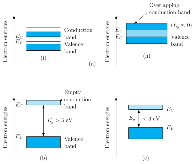
Energy bands: In an isolated atom electrons occupy discrete energy levels. When N atoms come together to form a solid, the atoms are so close that their electron wavefunctions overlap. By the Pauli exclusion principle each discrete level must split into N closely spaced sub-levels. As N is enormous, these sub-levels merge into essentially continuous ranges of allowed energy called energy bands, separated by forbidden gaps.
How they form: The highest band completely filled at 0 K is the valence band; the next higher (largely empty) band is the conduction band; between them lies the forbidden energy gap E_g. Only electrons in the conduction band (or in a partly filled band) can conduct electricity.
Distinction on the basis of band formation:
- Conductors (metals): the valence and conduction bands overlap, or the conduction band is partly filled, so E_g ≈ 0. Plenty of free electrons are always available → high conductivity.
- Semiconductors: a small forbidden gap, E_g ≈ 1 eV (Si ≈ 1.1 eV, Ge ≈ 0.7 eV). At 0 K they behave like insulators, but at room temperature some electrons are thermally excited across the gap → moderate, temperature-sensitive conductivity.
- Insulators: a large forbidden gap, E_g > 3 eV (e.g. diamond ≈ 6 eV). Electrons cannot be excited across it under ordinary conditions → practically no conduction.
OR (nuclear Q-value): For β⁺ (positron) emission 611C→511B+e++ν, using atomic masses the Q-value is
Q=[m(11C)−m(11B)−2me]c2.
…
Showing the 12 most recent of 24 on this concept.
- CBSE 2026Set ANNUAL1 markMCQQ.If the energy band gaps for Carbon, Silicon and Germanium are E1, E2 and E3 respectively, then the correct relation between them will be(a) E1 > E2 > E3(b) E1 = E2 = E3(c) E1 < E2 < E3(d) E1 > E2 < E3
›Reveal solutionSolution
Going from carbon (diamond) to silicon to germanium in Group 14, the energy band gap decreases, so E1 (carbon) > E2 (silicon) > E3 (germanium).
Carbon in its diamond form has a very wide energy gap (~5.4 eV), which is why it behaves as an insulator. Silicon has a moderate gap (~1.1 eV) and germanium has a smaller gap still (~0.7 eV), which is why both behave as semiconductors, with g …
- CBSE 2026Set ANNUAL1 markMCQQ.The width of forbidden band is maximum for(a) metals(b) non-conductors(c) semi-conductors(d) none of these
›Reveal solutionSolution
The forbidden gap (band gap) between valence and conduction bands is essentially zero for metals, small (~1 eV) for semiconductors, and large (>3 eV) for insulators.
In the band theory of solids, electrons occupy allowed energy bands, and the 'forbidden band' (band gap) is the energy range between the valence band (filled with electrons) and the conduction band (where electrons can move freely and conduct current).
- In METALS/conductors, the valence and conduction bands overlap (essentially zero gap), so electrons move into the conduction band with negligible energy input - hence high conductivity.
- In SEMICONDUCTORS, there is a small forbidden gap (of order 1 eV), so a modest amount of thermal or other energy can promote electrons across it. …
- CBSE 2026Set ANNUAL1 markQ.What do you understand by energy band?
›Reveal solutionSolution
In an isolated atom electrons occupy sharp, discrete energy levels; in a solid, the overlapping of countless such levels from ~10²³ closely packed atoms produces broad, continuous-looking bands of allowed energies.
In a single isolated atom, electrons can only have certain sharp, discrete energy values. When a huge number of atoms (of order Avogadro's number, ~1023 per cm³) are brought close together to form a solid, their outer electrons interact and each originally-discrete energy level splits into a large number of very closely spaced sub-levels — so close together that they appear to form a continuous range, called an energy band. The band formed from the valence electrons is the valence band, the next higher band (which may be empty or partly filled) is the conduction band, and the energy range between them where no allowed states exist is …
- CBSE 2025Set 55/4/11 markMCQQ.Which of the following is an electrical conductor at room temperature? (A) Sn (B) Mica (C) Si (D) C
›Reveal solutionSolution
The key idea is to classify each material by its electrical conductivity at room temperature. Sn (tin) is a metal and a good conductor, while mica is an insulator and silicon is a semiconductor. The correct option is (A).
Concept and Intuition
Electrical conductivity depends on how freely electrons can move through a material. At room temperature:
- Metals (like tin) have a "sea" of delocalized electrons that flow easily — they are excellent conductors.
- Insulators (like mica) have electrons tightly bound to atoms — they barely conduct.
- Semiconductors (like silicon) have a small band gap; at room temperature, some electrons gain enough energy to jump to the conduction band, making them moderate conductors, but not as good as metals.
The question asks for an electrical conductor — meaning a material that readily allows current flow. Among the options, only one is a metal.
Step-by-Step Solution
-
Identify the nature of each substance
- Sn (tin): A metal in Group 14 of the periodic table. It has metallic bonding with free electrons.
- Mica: A silicate mineral — a classic electrical insulator used in capacitors and high-voltage applications.
- Si (silicon): A metalloid, a semiconductor. Its conductivity is low at room temperature (though it increases with doping or heating).
- C (carbon): Can exist as graphite (a conductor) or diamond (an insulator). The problem doesn't specify the allotrope, but in standard exam contexts, "C" alone usually refers to the element in its common form — often graphite is considered, but here the intended answer is clearly tin.
-
Compare conductivities at room temperature
- Tin has a resistivity of about 1.1×10⁻⁷Ω⋅m — typical of a metal.
- Mica has resistivity exceeding 1012Ω⋅m — an insulator.
- Silicon has resistivity around 2.3×10³Ω⋅m — a semiconductor, not a good conductor at room temperature. …
- CBSE 2025Set X11 markMCQQ.The energy gap for silicon is :(a) 0.72 eV(b) 1.1 eV(c) 3 eV(d) 5 eV
›Reveal solutionSolution
(b) 1.1 eV The forbidden energy gap between the valence band and conduction band in silicon is about 1.1 eV at room temperature (for germanium it is about 0.72 eV). …
- CBSE 2025Set ANNUAL1 markMCQQ.The conduction band is partially empty in(a) non-conductors(b) semi-conductors(c) metals(d) super-conductors
›Reveal solutionSolution
Good conduction requires easily-available empty states just above the highest filled electron levels; in metals the conduction band itself is partially filled (or overlaps the valence band), giving electrons free states to move into under an applied field.
Band theory picture:
- Non-conductors (insulators): a large energy gap separates a full valence band from an empty conduction band, so essentially no electrons can be thermally excited across - conduction band stays effectively empty.
- Semiconductors: a small energy gap allows a few electrons to be thermally excited into an otherwise mostly-empty conduction band. …
- CBSE 2025Set ANNUAL1 markMCQQ.If temperature of semiconductor is fall, the forbidden energy gap is –(a) increased(b) remain unchanged(c) decreased(d) sometimes increased and sometimes decreased
›Reveal solutionSolution
The forbidden energy gap widens slightly as temperature falls.
For a semiconductor, the width of the forbidden energy gap Eg typically has a small, gradual dependence on temperature: as temperature falls, the band gap increases slightly (e.g. silicon's gap rises from about 1.12 eV at 300 K to about 1.17 eV near 0 K), mainly due to reduced thermal expansion and reduced electron-phonon interaction narrowing the gap les …
- CBSE 2025Set ANNUAL1 markMCQQ.The energy difference between valence band and conduction band of silicon at room temperature is about(a) 1.1 eV(b) 0.15 eV(c) 0.67 eV(d) 6.7 eV
›Reveal solutionSolution
Silicon's band gap at room temperature is about 1.1 eV, distinguishing it from germanium (~0.7 eV).
…
- CBSE 2025Set ANNUAL1 markQ.Distinguish between a semiconductor and an insulator based on their energy gap.
›Reveal solutionSolution
The energy gap between the valence and conduction bands is small enough in a semiconductor for thermal energy to promote a few electrons across it, but far too large in an insulator.
In the band theory of solids, electrical conduction requires electrons in the (otherwise full) valence band to be excited across the energy gap Eg into the empty conduction band.
- Semiconductor: Eg is small, typically about 1 eV or less (e.g. Si ≈1.1 eV, Ge ≈0.7 eV). At room temperature, thermal energy is enough to excite a small but significant number of electrons across this gap, giving the material a modest, temperature-dependent conductivity. …
- CBSE 2024Set A11 markQ.The value of energy band in insulators is ———————— than 3 eV. Fill in the blank choosing the appropriate answer from the bracket: (decreasing, interference, helium, greater, diffraction, increasing)
›Reveal solutionSolution
greater (more) than 3 eV. …
- CBSE 2024Set ANNUAL1 markMCQQ.Assertion (A): Resistance of conductors is lower than semiconductors. Reason (R): In conductors, energy gap between conduction band and valence band is greater than 3 eV.(a) Both A and R are correct and R is the correct explanation of A.(b) Both A and R are correct but R is not the correct explanation of A.(c) A is correct but R is incorrect.(d) Both A and R are incorrect.
›Reveal solutionSolution
Conductors do have lower resistance than semiconductors, but conductors have essentially zero (overlapping) energy gap, not a gap greater than 3 eV.
Assertion (A) is correct: conductors have much lower resistance (and much higher conductivity) than semiconductors, because conductors have a very large number of free charge carriers. Reason (R) is incorrect: in conductors, the conduction band and valence band actually overlap (energy gap Eg≈0) -- there is no forbidd …
- CBSE 2024Set A1 markMCQQ.The width of forbidden energy gap in the semiconductor is approximately (A) 1 eV (B) 10 eV (C) 100 eV (D) 0.01 eV
›Reveal solutionSolution
A semiconductor's forbidden energy gap is approximately 1 eV → option (A).
The energy gap between the top of the valence band and the bottom of the conduction band determines whether a material is a conductor, insulator or semiconductor. For semiconductors this gap is small, of the order of ~1 eV (e.g. ≈1.1 eV for silicon, ≈0.7 eV …
🎓Unlock everything free for 14 days
- ✓Full step-by-step solutions
- ✓Concept-first explanations
- ✓Methods, shortcuts & mistakes
- ✓PYQ mapping + timed mock tests
Full access for 14 days. No credit card required.