Q.What is P-N junction diode? Draw the circuit diagram for it in reverse bias mode. Draw V-I characteristic curve also.
You're viewing a preview — the full solution, concept, methods & PYQ mapping are locked.
Start your 14-day free trial to unlock the full solution →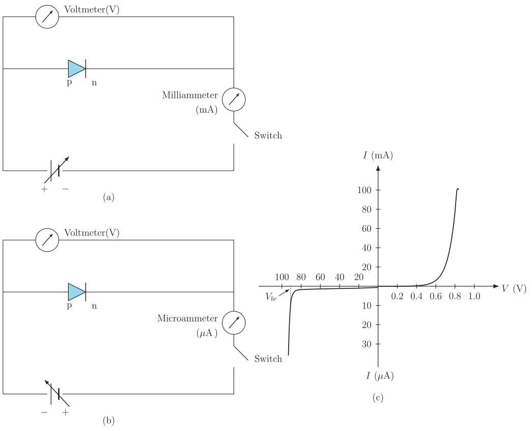
A P-N junction diode is formed by joining p-type and n-type semiconductor crystals; in reverse bias the depletion layer widens and only a small reverse current flows.
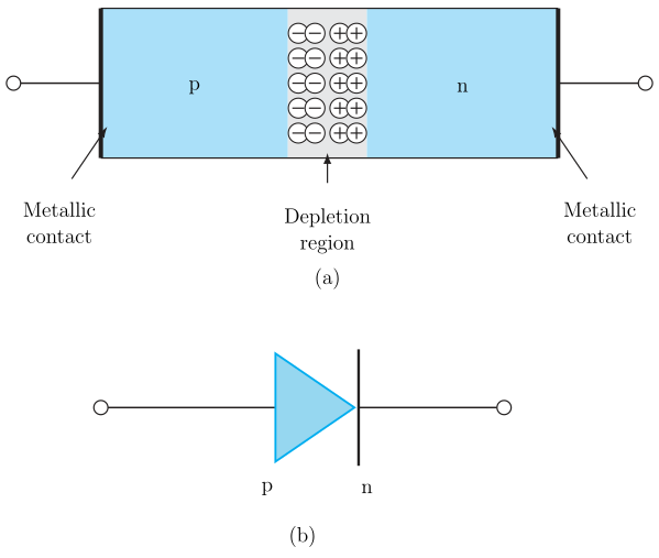
What is a P-N junction diode: It is a semiconductor device formed when a p-type semiconductor (majority carriers: holes) and an n-type semiconductor (majority carriers: free electrons) are joined together to form a single crystal with a junction between them. Near the junction, electrons and holes diffuse and recombine, leaving a narrow region depleted of mobile charge carriers called the depletion region, with an internal (built-in) potential barrier.
Circuit diagram — reverse bias: In reverse bias, the p-side of the diode is connected to the negative terminal of the battery and the n-side to the positive terminal (through a milliammeter/microammeter in series to measure the small reverse current, and a rheostat/potentiometer to vary the applied reverse voltage ):
Battery(+) ---- n-side | p-side ---- (µA meter) ---- Battery(−)
This polarity pulls the majority carriers further away from the junction, widening the depletion region and increasing the barrier, so almost no current flows except a very small reverse saturation current due to minority carriers.
…
Unlock everything free for 14 days
- Full step-by-step solutions
- Concept-first explanations
- Methods, shortcuts & mistakes
- PYQ mapping + timed mock tests
Full access for 14 days. No credit card required.