Question of 37
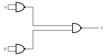
Q.Identify the logic gates marked P and Q. Rewrite the truth table with output Y for input conditions shown in the truth table for the combination of logic gates and identify the logic operation carried out by the combination of gates. OR A semiconductor X is made by doping a germanium crystal with indium. A second semiconductor Y is made by doping germanium with arsenic. The two are joined end to end and connected to a battery as shown (a diagram shows blocks X and Y joined in series and connected to a battery) :
(i) Identify the semiconductors X and Y obtained after doping.
(ii) Identify the biasing and draw VI characteristics.
(iii) If the polarity of the source is reversed, how will the width of the depletion region change ?
Goa GbshseGBSHSE Class 12 Board Exam 2024Subjective· 4mImportance★★★★★
0% · 0/37 Questions
You're viewing a preview — the full solution, concept, methods & PYQ mapping are locked.
Start your 14-day free trial to unlock the full solution →Two NOT gates followed by a NAND gate is, by De Morgan's theorem, equivalent to an OR gate.
From the circuit, input A passes through a single-input gate P before reaching the next gate, and input B passes through an identical gate P — a single-input gate that inverts its input is a NOT gate. The outputs of the two NOT gates (i.e. and ) feed into a two-input gate Q whose output is Y — a gate producing is a NAND gate.
Truth table:
| A | B | ||||
|---|---|---|---|---|---|
| 0 | 0 | 1 | 1 | 1 | 0 |
| 0 | 1 | 1 | 0 | 0 | 1 |
| 1 | 0 | 0 | 1 | 0 | 1 |
Unlock everything free for 14 days
- Full step-by-step solutions
- Concept-first explanations
- Methods, shortcuts & mistakes
- PYQ mapping + timed mock tests
Full access for 14 days. No credit card required.