Question of 37
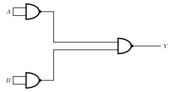
Q.In the figure shown below :
(a) Identify the gates P and Q.
(b) Write the truth table for inputs A and B and output Y.
(c) Identify the logic operation carried out with the combination of gates.
OR
How can you convert a NAND gate into a :
(i) NOT gate
(ii) AND gate
(iii) OR gate. Write the necessary truth tables and draw the necessary diagrams.
Goa GbshseGBSHSE Class 12 Board Exam 2025Subjective· 4mImportance★★★★★
0% · 0/37 Questions
You're viewing a preview — the full solution, concept, methods & PYQ mapping are locked.
Start your 14-day free trial to unlock the full solution →Tracing each gate's truth table through the network shows the NAND-NOR-NOR combination reduces exactly to - this circuit is a roundabout way of building an AND gate from NAND/NOR gates.
- Identification: Gate P is drawn AND-shaped with a bubble on its output, so it is a NAND gate, giving . Gate Q is drawn OR-shaped (curved back) with a bubble on its output, so it is a NOR gate, giving . The third gate is also OR-shaped with a bubble on its output, taking and as its two inputs, so it is also a NOR gate, giving .
- Truth table:
| A | B | A' = NAND(A,B) | B' = NOR(A,B) | Y = NOR(A',B') |
|---|---|---|---|---|
| 0 | 0 | 1 | 1 | 0 |
| 0 | 1 | 1 | 0 | 0 |
| 1 | 0 | 1 | 0 | 0 |
| 1 | 1 | 0 | 0 | 1 |
| … |
Unlock everything free for 14 days
- Full step-by-step solutions
- Concept-first explanations
- Methods, shortcuts & mistakes
- PYQ mapping + timed mock tests
Full access for 14 days. No credit card required.