Electronics · Ch 11 — Microcontroller
Assembly Language Programming, Arithmetic Operations and the PIC Microcontroller
Assembly Language Programming, Arithmetic Operations and the PIC Microcontroller
Assembly language programming (ALP)
Programming resembles writing fiction: the science lies in the rules (grammar, structure), the art in how the pieces are arranged. A computer carries out a series of binary operations — storing and retrieving data, adding, subtracting and applying Boolean logic — and the ordered sequence of such operations is a computer program. The program is executed inside the CPU but is itself stored in system memory, not in the CPU.
Programs live in memory, of which there are three broad types:
- ROM (Read Only Memory): non-volatile; its contents cannot be changed by the CPU during normal running.
- RAM (Random Access Memory): read/write and volatile (contents are lost when power is removed); includes static RAM (SRAM) and dynamic RAM (DRAM).
- Hybrid memory (EEPROM — Electrically Erasable and Programmable Read Only Memory): can be written like RAM yet keeps its contents when power is removed.
Every instruction is made of an opcode (the "verb", the operational code that says what to do) and an operand (the "noun", the data acted on). Code memory holds the program, while data addresses are the memory locations the CPU reads and writes under program control, whose contents are data numbers. Machine language is pure binary code — not readable by people — while assembly language is the human-friendly bridge, written as instruction mnemonics and translated to machine code by assembling.
Programmers choose assembly language to gain: 1. speed, 2. a smaller program size, 3. the ability to handle special situations, 4. lower cost, and 5. a better understanding of how the computer actually works. Being a low-level language, assembly deals directly with the CPU's internal structure, and writing it needs a few utility tools: 1. an operating system, 2. a word processor or text editor, 3. an assembler, and 4. a testing program. Three registers the programmer must know are register A (the accumulator, 8 bits / 1 byte), register R (temporary storage, 8 bits) and the register PC / Program Counter (holds the address of the next instruction, 16 bits / 2 bytes, so code addresses run from 0000H to FFFFH — a 64 KB limit).
Structure of an assembly language program
An assembly program is a series of lines; each instruction is a mnemonic followed by one or two operands (the data being manipulated). It is important to separate instructions — such as ADD or MOV, which are commands to the CPU — from directives (also called pseudo-instructions) — such as ORG and END, which are directions to the assembler. ORG tells the assembler where to place the opcode (for example at memory location 0), and END marks the end of the source code. An assembly instruction has four fields, laid out as:
[label:] mnemonic [operands] [; comment]
where the square brackets show optional fields that are not actually typed (for example ADD A,B or MOV A,#51).
A sample assembly language program
The short program below loads two numbers, clears the accumulator and adds the numbers (and a constant) into A, then parks the CPU in a tight loop:
        ORG 0H          ; start at location 0
        MOV R2,#15H     ; load 15H into R2
        MOV R6,#23H     ; load 23H into R6
        MOV A,#0        ; clear the accumulator
        ADD A,R2        ; A = A + R2
        ADD A,R6        ; A = A + R6
        ADD A,#10H      ; A = A + 10H
HERE:   SJMP HERE       ; stay in this loop
        END             ; end of the source file
Assembling and running an 8051 program
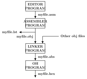
Turning source code into something the chip can run takes a small toolchain (Figure 11.2.1). The steps are:
- An editor (such as MS-DOS EDIT or Windows Notepad) is used to type the program, producing an ASCII source file with the extension
.asm(sometimes.src). - The source file is fed to an 8051 assembler, which converts the instructions to machine code and produces an object file (
.obj) and a list file (.lst). - Linking — the linker takes one or more object files and produces an absolute object file (
.abs), the form used by 8051 trainers that run a monitor program. - The
.absfile is passed to an OH (object-to-hex) program, which creates the.hexfile that is finally burned into ROM.
The .lst file is optional but useful: it lists all the opcodes, their ROM addresses and any errors the assembler found. Table 11.2.1 shows a worked list-file example.
Arithmetic operations on the 8051
The 8051's arithmetic is done through the accumulator. Four operations are studied.
1. Addition — ADD A,source computes A = A + source; the destination is always register A, while the source may be a register, immediate data or a memory byte. Memory-to-memory arithmetic is never allowed in 8051 assembly. Additions set the flags: a carry out of bit-7 sets CY, and a carry from bit-3 to bit-4 sets the auxiliary carry AC (the flag/accumulator bits D7-D0 are shown in the byte-layout figure below). For example, adding 1FH and 5EH gives 7DH (0001 1111 + 0101 1110 = 0111 1101).
2. Subtraction — the 8051 has only SUBB (subtract with borrow). To do a plain subtraction you must first clear the carry (CLR C, so CY = 0) before SUBB. The chip subtracts using the 2's-complement method: it takes the 2's complement of the source (the subtrahend), adds it to A (the minuend), and inverts the carry. After a SUBB, CY = 0 means the result is positive and CY = 1 means it is negative (with the destination holding the 2's complement of the true result). Recall that the 2's complement is obtained by taking the 1's complement (CPL) and then incrementing (INC).
3. Multiplication — unsigned multiplication uses MUL AB (note: there is no comma between A and B). Both A and B serve as source and destination: A × B gives a 16-bit result whose low byte goes to A and high byte to B. For example 35H × 45H = 0E49H (B = 0EH, A = 49H). Table 11.2.2 summarises this.
4. Division — unsigned division uses DIV AB and works byte-over-byte only. The numerator must be in A and the denominator in B; after the operation the quotient is in A and the remainder in B. If B = 0 the operation is invalid and the OV flag is set to 1; otherwise DIV clears both CY and OV. For example 85 ÷ 10 gives quotient 08 in A and remainder 05 in B. Table 11.2.3 summarises this.
As explained in Section 11.1, the printed book frequently prints the hex digit 0 as the letter "O" (for example "OF1H", "ODH" and "ORG OH") and sometimes prints the hex suffix H as "M". The correct forms are 0F1H, 0DH, ORG 0H and the suffix H; these are the values used above.
The PIC microcontroller — introduction
The PIC is a family of microcontroller chips made by Microchip Technology of Chandler, Arizona. The name PIC stands for Peripheral Interface Controller. A PIC is a powerful, fully featured processor with its own internal RAM, EEPROM/flash memory and peripherals, and it is very popular with hobbyists and experimenters in electronics and robotics because it is widely available, low in cost, easy to program (with built-in EEPROM), well documented with application notes, and supported by plenty of development tools; it is often branded "PICmicro". If the main CPU is like the brain, a PIC is like the autonomic nervous system that quietly runs background tasks. The PIC was designed around 1980 (by General Instrument) as a small, fast, inexpensive embedded controller with strong I/O. Nearly all of its instructions execute in the same number of clock cycles, which makes timing easy to predict, and it uses a RISC (Reduced Instruction Set Computer) design whose efficient code needs less program memory than larger rivals.
Core features of the PIC
Nine features explain the PIC's popularity:
- Integration of operational features — power-on reset and brown-out protection keep the chip running only while the supply is within specification; a watchdog timer resets the PIC if it misbehaves; four selectable clock oscillators (from a low-cost RC oscillator to a high-accuracy crystal) and several low-power options are available.
- Instruction-set simplicity — just 35 instructions.
- Speed — at maximum clock rate most instructions execute in about 0.2 µs, i.e. roughly five instructions per microsecond.
- Powerful output-pin control — a single instruction can drive one output pin high or low in about 0.2 µs, and a pin can source or sink a load of up to 25 mA.
- Interrupt control — up to 12 independent interrupt sources.
- Programmable timer options — three versatile timers characterise inputs, control outputs and provide internal timing.
- Serial programming via two pins — PIC programmers are available for under 100 US dollars.
- EPROM / OTP / ROM options — UV-erasable EPROM parts for development and one-time-programmable (OTP) parts for production.
- I/O port expansion — the built-in serial peripheral interface can use standard 16-pin shift-register ports to add any number of I/O pins.
The feature table for this topic is given below (Feature / Description).
Limitations of the PIC
Against these strengths the PIC has a few limitations: it has only one accumulator; register-bank switching is needed to reach the whole RAM of many devices; and its operations and registers are not orthogonal — some instructions can address RAM and/or immediate constants, while others can work only through the accumulator.
Overview of the PIC16F887 …
Assembly language is a human-readable, low-level programming language written as instruction mnemonics that map directly onto a CPU's machine instructions. It is translated in …
Machine language is the binary-coded form of a program that the CPU executes directly. It is not readable by people, which is why programmers write in assembly language and let an as …
EEPROM (Electrically Erasable and Programmable Read Only Memory) is a hybrid memory: it can be written to like RAM, yet it keeps its stored bits even when power is removed, like ROM. Unlike volatile RAM its contents survive a power-down, and unlike plain ROM it can be rewritten by the CPU, so it holds data that mu …
A directive, such as ORG or END, is a command to the assembler rather than to the CPU. ORG fixes where the following code is placed in memory; END marks the end of the source file. A directive produce …
Drawn by us to help you understand the concept clearly, and verified to make sure it's accurate. For exams, practice from your textbook's own diagram.
Shows the sequence that turns source code into a burnable file: EDITOR PROGRAM produces myfile.asm; ASSEMBLER PROGRAM produces myfile.lst and myfile.obj; the LINKER PROGRAM (which may also take other object files) produces myfile.abs; and the OH PROGRAM produces myfile.hex. Matches t …
| No. | ROM address | Machine language | Assembly language | Comment |
|---|---|---|---|---|
| 1 | 0000 | ORG 0H | ; start at location 0 | |
| 2 | 0000 | 7D25 | MOV R5,#25H | ; load 25H into R5 |
| 3 | 0002 | 7F34 | MOV R7,#34H | ; load 34H into R7 |
| 4 | 0004 | 7400 | MOV A,#0 | ; load 0 into A |
| 5 | 0006 | 2D | ADD A,R5 | ; A = A + R5 |
| 6 | 0007 | 2F | ADD A,R7 | ; A = A + R7 |
| 7 | 0008 | 2412 | ADD A,#12H | ; A = A + 12H |
| 8 | 000A | 80FE | HERE: SJMP HERE | ; stay in this loop |

Drawn by us to help you understand the concept clearly, and verified to make sure it's accurate. For exams, practice from your textbook's own diagram.
Illustrates the eight bit positions D7 to D0 of an 8-bit register so that carries generated during addition can be traced: a carry out of D7 sets the carry flag CY, and a carry from D3 to D4 sets the auxiliary-carry flag AC. Matches the textbook's D7-D0 flag-regi …
ADD A, source performs A = A + source. The destination is always the accumulator A; the source may be a register, immediate data or a memory byte. Memory-to-memory arithme …
The 8051 subtracts only with borrow: SUBB A, source gives A = A − source − CY. For a plain subtraction, clear the carry first with CLR C. Subtraction is performed internally by 2's-complement addition; afterwards CY = 0 indicates a positive result and CY = 1 a negative one. The 2's complement …
MUL AB multiplies the unsigned bytes in A and B: A × B gives a 16-bit product whose low byte is left in A and high byte in B. There is no comma between A and B. Both A and B serve as source and destination, and only unsigned multiplication is directly supported. For example 35H × 45H = 0E49H …
DIV AB divides the unsigned byte in A by the unsigned byte in B: the quotient is left in A and the remainder in B. If B = 0 the result is invalid and the OV flag is set to 1; …
| Multiplication | Operand 1 | Operand 2 | Result |
|---|---|---|---|
| Byte × byte | A | B | A = low byte, B = high byte |
| Division | Numerator | Denominator | Quotient | Remainder |
|---|---|---|---|---|
| byte / byte | A | B | A | B |
A PIC (Peripheral Interface Controller) is a family of RISC microcontrollers from Microchip Technology, combining a CPU with internal RAM, EEPROM/flash memory and peripherals. It is widely used in embedded control, hobby electronics and robotics because it …
| Feature | Description |
|---|---|
| Flash memory | Re-programmable program storage |
| RAM | Memory storage for variables |
| EEPROM | Long-term stable memory |
| I/O ports | High-current input/output ports (with pin-direction change) |
| Timers/Counters | Typically 3 |
| ADC | Analogue-to-digital converter |
| PSP | Parallel Slave Port (for 8-bit microprocessor systems) |
| LCD | LCD interface |
Drawn by us to help you understand the concept clearly, and verified to make sure it's accurate. For exams, practice from your textbook's own diagram.
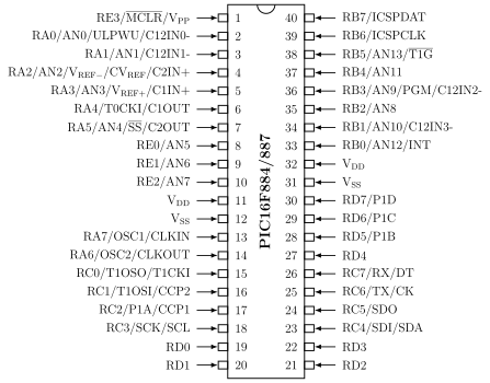
Shows the PIC16F884/887 in a 40-pin PDIP package with each pin's multiplexed functions — analog inputs AN0-AN13, comparator inputs, timer inputs, CCP/PWM, serial and in-circuit-serial-programming functions, the MCLR/Vpp reset pin and the VDD/VSS supply pins. Matches the textbook's PIC16F884 …