Electronics · Ch 11 — Microcontroller
The 8051 Microcontroller — Architecture, Addressing Modes and Instruction Set
The 8051 Microcontroller — Architecture, Addressing Modes and Instruction Set
The microprocessor
A microprocessor is the general-purpose Central Processing Unit (CPU) of a digital computer. By itself it is not a complete computer — it only does the processing and needs external memory and I/O to become useful. Its internal block diagram (Figure 11.1.1) contains an Arithmetic and Logic Unit (ALU), a Program Counter (PC), a Stack Pointer (SP), one or more working registers, a clock-timing circuit and interrupt circuits.
Function of each block:
- Arithmetic and Logic Unit (ALU): performs arithmetic operations and takes logical decisions.
- Accumulator: stores a number; when a second number arrives it adds the two and stores the sum. It can also sense a signal, and clear or complement its contents.
- Working register(s): a short-term store of one word, often a group of flip-flops.
- Program Counter (PC): holds the address of a byte in memory and points to the next instruction to be fetched and executed.
- Stack Pointer (SP): holds an address in internal RAM; used with certain opcodes to store and retrieve data quickly.
- Clock circuit: generates the clock pulses that synchronise all internal operations.
- Interrupt circuits: break the normal program flow and later allow it to resume from the same point.
The microcontroller and its blocks
A microcontroller is a true "computer on a chip". It has every feature of a microprocessor and, in addition, on-chip ROM, RAM, parallel I/O, serial I/O, timers/counters and a clock circuit. Its block diagram (Figure 11.1.2) shows these blocks: ALU; accumulator and register(s); internal RAM (holds the programs the user loads); stack pointer (holds an internal-RAM address); timer/counter (counts internal or external pulses); internal ROM (program memory, holds the fixed program); program counter; I/O port circuits (connect the chip to the outside world); interrupt circuits; and clock circuits.
Comparison between microprocessor and microcontroller
The two devices differ chiefly in what is on the chip and what the designer must add externally. The book's Table 11.1.1 sets them side by side (see the comparison table below).
The 8051 microcontroller
The 8051 is an 8-bit microcontroller with 128 bytes of RAM, 4 KB of on-chip ROM, two timers, one serial port and four 8-bit ports, all on a single chip. Two other members of the same family are the 8052 and the 8031. Its key feature quantities are collected in Table 11.1.2 (see below).
Architecture of the 8051
The 8051 block diagram (Figure 11.1.3) brings together the features that make it a microcontroller: internal ROM and RAM, I/O ports with programmable pins, timers/counters, serial data communication, a program counter, an ALU, working registers and clock circuits. In more detail the 8051 has:
- a 16-bit Program Counter;
- 4 KB of internal ROM or EPROM;
- an 8-bit CPU with registers A (accumulator) and B;
- 128 bytes of internal RAM;
- 32 I/O pins arranged as four 8-bit ports, P0-P3;
- two 16-bit timer/counters, T0 and T1;
- two external and three internal interrupt sources;
- oscillator and clock circuits;
- the control registers TCON, TMOD, SCON, PCON, IP and IE;
- a CISC (Complex Instruction Set Computer) architecture.
The 40-pin DIP pin configuration is shown in Figure 11.1.4, where pin numbers are printed inside the package and pin names outside. Many Port-3 pins carry alternate functions (for example RXD/TXD for the serial port on P3.0/P3.1, the external-interrupt inputs INT0/INT1 on P3.2/P3.3, the timer inputs T0/T1 on P3.4/P3.5, and the WR/RD strobes on P3.6/P3.7), while Port-0 and Port-2 double as the multiplexed address/data bus.
The printed textbook describes the 32 I/O pins as "48-bit ports"; this is a misprint. The 8051 actually has four 8-bit ports (4 × 8 = 32 pins), namely P0, P1, P2 and P3. The correct description is used throughout this material.
Addressing modes
Because the CPU can keep data in registers, in memory or in an external source, an instruction can reach its data in several ways. The rules that describe how an operand is located are called addressing modes. In 8051 instructions the destination address is written first, followed by the source. The 8051 has five addressing modes: (1) register, (2) direct, (3) immediate, (4) indirect, and (5) base register plus index register; the first four are the ones commonly used. There are 28 opcodes that simply copy data from a source to a destination; the three main data-move opcodes are MOV destination,source; PUSH source / POP destination; and XCH destination,source. The MOV family moves data within the four physical parts of 8051 memory — internal RAM, internal Special Function Registers (SFRs), external RAM, and internal/external ROM — using the opcodes MOV, MOVX, MOVC, PUSH/POP and XCH.
1. Register addressing mode — registers A, DPTR, R0-R7, the accumulator and the carry bit appear as part of the opcode mnemonic, as the source or the destination. Moves happen between A and R0-R7, e.g. MOV A,R0 (copy R0 into A), MOV R2,A (copy A into R2), ADD A,R5 (add R5 to A) and MOV R5,A (save A in R5). The three least-significant bits of the opcode select which register is used (Table 11.1.3 shows this for MOV A,R7). A MOV never alters the source; it only copies.
2. Direct addressing mode — the whole 128 bytes of internal RAM and the SFRs can be addressed directly by a single-byte address. Internal RAM uses addresses 00H-7FH; the SFRs occupy 80H-FFH. The instruction MOV A,direct carries an opcode byte followed by the 8-bit direct address, and the on-chip memory map is shown in Figure 11.1.5. RAM addresses 00H-1FH are also the four banks of eight working registers R0-R7, so, for example, R2 of bank 2 can be reached in register mode as R2 or in direct mode as address 12H. The SFR addresses are listed in Table 11.1.4 and the register-bank direct addresses in Table 11.1.5. Worked instructions include MOV R0,40H, MOV 56H,A, MOV 80H,A (the same as MOV P0,A, because P0 is address 80H), MOV A,4 (the same as MOV A,R4) and MOV 0F0H,R2 (the same as MOV B,R2).
3. Indirect addressing mode — a register acts as a pointer to the data. For data inside the CPU only R0 and R1 may be used as pointers (R2-R7 cannot), and when used this way they must be preceded by the @ sign. Examples: MOV A,@R0 (copy the RAM byte whose address is in R0 into A), MOV @R1,B (copy B into the RAM byte whose address is in R1) and MOV @R1,90H. Figure 11.1.6 shows the internal 128 bytes of RAM (the upper 128 bytes, 80H-FFH, exist only on the 8032/8052).
4. Immediate addressing mode — the data itself is made part of the opcode, so it is immediately available within the instruction. A # sign marks immediate data, e.g. MOV A,#25H, MOV R4,#62, MOV DPTR,#4562H (16-bit) and MOV R7,#06H (8-bit). When the 8051 executes an immediate move, the program counter automatically advances to the byte(s) following the opcode.
5. Base register plus index register addressing mode — an effective address is formed by adding an index register to a base register (used with instructions such as MOVC A,@A+DPTR), giving a flexible way to reach look-up tables held in code memory.
Throughout this chapter the printed book very often typesets the hexadecimal digit 0 (zero) as the capital letter "O" — for example it prints "ORG OH" for ORG 0H, and "OF1H" for 0F1H. It also prints the Special Function Registers IE (Interrupt Enable) and IP (Interrupt Priority) as "1E" and "1P" in its SFR table. These are print errors: hexadecimal numbers use the digit 0, and the standard register names are IE and IP. The correct forms are used here.
The 8051 instruction set
When a program runs it often has to hand control to a different location, so the 8051 provides a rich instruction set — 111 instructions in all — grouped into four categories: 1. data transfer, 2. arithmetic, 3. logical and 4. program-branching instructions. Every instruction is written as a mnemonic followed by a destination operand and a source operand (the "8051 instruction format").
Data-transfer instructions (MOV, MOVX, MOVC, PUSH, POP and the exchange instructions XCH/XCHD) move data about. They do not affect the PSW flags, except that a MOV or POP written directly to PSW can change the flags. Flags are 1-bit registers that record the result of certain instructions; they are gathered inside the Program Status Word (PSW) and Power Control (PCON) registers so they can be addressed conveniently. The stack instructions PUSH and POP name a direct address and move data to or from an internal-RAM area called the stack; the Stack Pointer (SP) holds the RAM address involved. A PUSH add first increments SP and then copies the byte at add into the RAM location pointed to by SP; a POP add copies the byte from the RAM location in SP back to add and then decrements SP (Figure 11.1.7). The exchange instructions move data both ways at once and always involve register A (for example XCH A,Rn, XCH A,add and XCH A,@R1); every addressing mode except immediate may be used. The complete list is Table 11.1.6. …
A microprocessor is the general-purpose Central Processing Unit (CPU) of a digital computer. It performs the processing but is not a complete computer by itself — it must be given external …
A microcontroller is a complete computer on a single chip. It contains a CPU together with on-chip ROM, RAM, parallel and serial I/O, timers/counters, and interrupt and clock circuits, so it can run a fixed appli …
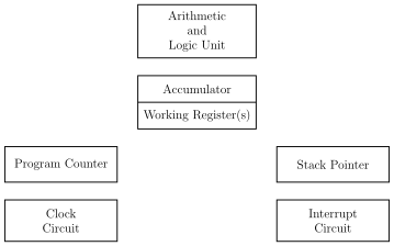
Drawn by us to help you understand the concept clearly, and verified to make sure it's accurate. For exams, practice from your textbook's own diagram.
Depicts the internal organisation of a microprocessor CPU as separate blocks — ALU, accumulator over working register, program counter, stack pointer, clock circuit and interrupt circuit — making the point that a microprocessor is only the processing core and needs external memory and I/O. Matches …
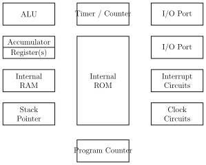
Drawn by us to help you understand the concept clearly, and verified to make sure it's accurate. For exams, practice from your textbook's own diagram.
Shows the microcontroller as a single chip carrying every block a small computer needs — ALU, accumulator and register(s), internal RAM, stack pointer, timer/counter, internal ROM, program counter, I/O ports, interrupt circuits and clock circuits. Matches the t …
| Microprocessor | Microcontroller |
|---|---|
| Contains ALU, program counter, stack pointer, working registers, interrupt circuits and a clock-timing circuit. | Contains ALU, PC, SP, register, ROM, RAM, parallel I/O, serial I/O, counters and a clock circuit. |
| A designer using a general-purpose microprocessor must add RAM, ROM, I/O ports and a timer externally to make it functional. | All are embedded together on the chip, so the designer cannot add any external memory, I/O or timer. |
| Most microprocessors have many opcodes for moving data from external memory to the CPU. | Microcontrollers have one or two. |
| A microprocessor may have one or two types of bit-handling instruction. | Microcontrollers have many. |
| The microprocessor is concerned with rapid movement of code and data from external addresses to the chip. | The microcontroller is concerned with rapid movement of bits within the chip. |
| Feature | Quantity |
|---|---|
| ROM | 4 KB |
| RAM | 128 bytes |
| Timer | 2 |
| I/O pins | 32 |
| Serial port | 1 |
| Interrupt sources | 6 |
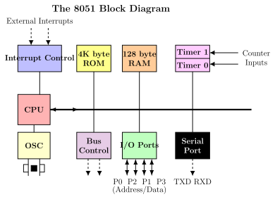
Drawn by us to help you understand the concept clearly, and verified to make sure it's accurate. For exams, practice from your textbook's own diagram.
Shows the internal architecture of the 8051: the CPU and interrupt control, 4 KB ROM, 128 bytes RAM, Timer 0 and Timer 1, the oscillator, bus control, the four I/O ports P0-P3 (also the address/data bus) and the serial port (TXD/RXD), all tied to one internal bus. Matches the …
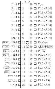
Drawn by us to help you understand the concept clearly, and verified to make sure it's accurate. For exams, practice from your textbook's own diagram.
Shows the 8051 as a 40-pin DIP: the left side carries P1.0-P1.7, RST, Port-3 (with alternate functions RXD, TXD, INT0, INT1, T0, T1, WR, RD), XTAL2, XTAL1 and GND; the right side carries Vcc, Port-0 (AD0-AD7), EA/Vpp, ALE/PROG, PSEN and Port-2 (A8-A15). Pin numbers are printed inside the package and names outside. Mat …
An addressing mode is the way an instruction specifies where its operand is located. Because data may sit in a register, in memory or in an external source, the addressing mode defines how that source is reached. The 8051 has five modes: register, direct, immediate, …
The single-byte opcode for MOV A,R7. The five most-significant bits are the opcode part and the three least-significant bits select the register:
| Bit | b7 | b6 | b5 | b4 | b3 | b2 | b1 | b0 |
|---|---|---|---|---|---|---|---|---|
| Value | 1 | 1 | 1 | 0 | 1 | 1 | 1 | 1 |
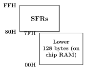
Drawn by us to help you understand the concept clearly, and verified to make sure it's accurate. For exams, practice from your textbook's own diagram.
Shows the memory a direct address can reach: the Special Function Registers occupy 80H-FFH and sit above the lower 128 bytes of on-chip RAM, which run 00H-7FH. Matches the textbook's Figu …
| SFR | Direct address (hex) | Bit addresses (hex) |
|---|---|---|
| A | 0E0H | 0E0-0E7 |
| B | 0F0H | 0F0-0F7 |
| DPL | 82H | — |
| DPH | 83H | — |
| IE | 0A8H | 0A8-0AF |
| IP | 0B8H | 0B8-0BF |
| P0 | 80H | 80-87 |
| P1 | 90H | 90-97 |
| P2 | 0A0H | 0A0-0A7 |
| P3 | 0B0H | 0B0-0B7 |
| PCON | 87H | — |
| PSW | 0D0H | 0D0-0D7 |
| SBUF | 99H | — |
| SCON | 98H | 98-9F |
| SP | 81H | — |
| TCON | 88H | 88-8F |
| TMOD | 89H | — |
| TH0 | 8CH | — |
| TL0 | 8AH | — |
| TH1 | 8DH | — |
| TL1 | 8BH | — |
| Bank | R0 | R1 | R2 | R3 | R4 | R5 | R6 | R7 |
|---|---|---|---|---|---|---|---|---|
| 0 | 00H | 01H | 02H | 03H | 04H | 05H | 06H | 07H |
| 1 | 08H | 09H | 0AH | 0BH | 0CH | 0DH | 0EH | 0FH |
| 2 | 10H | 11H | 12H | 13H | 14H | 15H | 16H | 17H |
| 3 | 18H | 19H | 1AH | 1BH | 1CH | 1DH | 1EH | 1FH |
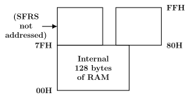
Drawn by us to help you understand the concept clearly, and verified to make sure it's accurate. For exams, practice from your textbook's own diagram.
Shows the internal 128 bytes of RAM that register-indirect addressing (@R0/@R1) can reach, and marks the upper 128 bytes (80H-FFH) as present only on the 8032/8052, with the SFR space not reachable by indirect addressing. Matches the textb …
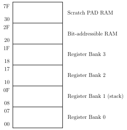
Drawn by us to help you understand the concept clearly, and verified to make sure it's accurate. For exams, practice from your textbook's own diagram.
Shows how the 128 bytes of 8051 internal RAM are organised: the four register banks R0-R7 occupy 00H-1FH (bank 1, 08H-0FH, doubles as the default stack), the bit-addressable area is 20H-2FH, and the general-purpose scratch-pad RAM is 30H-7FH. This underpins register and direct addressing. Matches the textbook's ch …
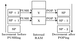
Drawn by us to help you understand the concept clearly, and verified to make sure it's accurate. For exams, practice from your textbook's own diagram.
Illustrates stack operation: on a PUSH the stack pointer is first incremented and the byte is written into internal RAM; on a POP the byte is read from the RAM location in SP and the stack pointer is then decremented. Matches the textbo …
| Mnemonic | Description | Byte | Oscillator period |
|---|---|---|---|
| MOV A,Rn | Move register to accumulator | 1 | 12 |
| MOV A,direct | Move direct byte to accumulator | 2 | 12 |
| MOV A,@Ri | Move indirect RAM to accumulator | 1 | 12 |
| MOV A,#data | Move immediate data to accumulator | 2 | 12 |
| MOV Rn,A | Move accumulator to register | 1 | 12 |
| MOV Rn,direct | Move byte to register | 2 | 24 |
| MOV direct,direct | Move direct byte to direct | 3 | 24 |
| MOV DPTR,#data16 | Load data pointer with a 16-bit constant | 3 | 24 |
| MOV A,@A+DPTR | Move code byte relative to DPTR to accumulator | 1 | 24 |
| MOV A,@A+PC | Move code byte relative to PC to accumulator | 1 | 24 |
| MOVX A,@Ri | Move external RAM (8-bit address) to accumulator | 1 | 24 |
| MOVX @Ri,A | Move accumulator to external RAM (8-bit address) | 1 | 24 |
| MOVX @DPTR,A | Move accumulator to external RAM (16-bit address) | 1 | 24 |
| PUSH direct | Push direct byte onto stack | 2 | 24 |
| POP direct | Pop direct byte from stack | 2 | 24 |
| XCH A,Rn | Exchange register with accumulator | 1 | 12 |
| XCH A,@Ri | Exchange indirect RAM with accumulator | 1 | 12 |
| XCHD A,@Ri | Exchange low-order nibble of indirect RAM with accumulator | 1 | 12 |
| Mnemonic | Description | Byte | Oscillator period |
|---|---|---|---|
| ADD A,Rn | Add register to accumulator | 1 | 12 |
| ADD A,direct | Add direct byte to accumulator | 2 | 12 |
| ADD A,@Ri | Add indirect RAM to accumulator | 1 | 12 |
| ADD A,#data | Add immediate data to accumulator | 2 | 12 |
| ADDC A,Rn | Add register to accumulator with carry | 1 | 12 |
| ADDC A,direct | Add direct byte to accumulator with carry | 2 | 12 |
| ADDC A,@Ri | Add indirect RAM to accumulator with carry | 1 | 12 |
| ADDC A,#data | Add immediate data to accumulator with carry | 2 | 12 |
| SUBB A,Rn | Subtract register from accumulator with borrow | 1 | 12 |
| SUBB A,direct | Subtract direct byte from accumulator with borrow | 2 | 12 |
| SUBB A,@Ri | Subtract indirect RAM from accumulator with borrow | 1 | 12 |
| SUBB A,#data | Subtract immediate data from accumulator with borrow | 2 | 12 |
| INC A | Increment accumulator | 1 | 12 |
| INC Rn | Increment register | 1 | 12 |
| INC direct | Increment direct byte | 2 | 12 |
| INC @Ri | Increment indirect RAM | 1 | 12 |
| DEC A | Decrement accumulator | 1 | 12 |
| DEC Rn | Decrement register | 1 | 12 |
| DEC direct | Decrement direct RAM | 2 | 12 |
| DEC @Ri | Decrement indirect RAM | 1 | 12 |
| Mnemonic | Description | Byte | Oscillator period |
|---|---|---|---|
| ANL A,Rn | AND register to accumulator | 1 | 12 |
| ANL A,direct | AND direct byte to accumulator | 2 | 12 |
| ANL A,@Ri | AND indirect RAM to accumulator | 1 | 12 |
| ANL A,#data | AND immediate data to accumulator | 2 | 12 |
| ANL direct,A | AND accumulator to direct byte | 2 | 12 |
| ANL direct,#data | AND immediate data to direct byte | 3 | 24 |
| ORL A,Rn | OR register to accumulator | 1 | 12 |
| ORL A,direct | OR direct byte to accumulator | 2 | 12 |
| ORL A,@Ri | OR indirect RAM to accumulator | 1 | 12 |
| ORL A,#data | OR immediate data to accumulator | 2 | 12 |
| ORL direct,A | OR accumulator to direct byte | 2 | 12 |
| ORL direct,#data | OR immediate data to direct byte | 3 | 24 |
| XRL A,Rn | Exclusive-OR register to accumulator | 1 | 12 |
| XRL A,direct | Exclusive-OR direct byte to accumulator | 2 | 12 |
| XRL A,@Ri | Exclusive-OR indirect RAM to accumulator | 1 | 12 |
| XRL A,#data | Exclusive-OR immediate data to accumulator | 1 | 12 |
| XRL direct,A | Exclusive-OR accumulator to direct byte | 2 | 12 |
| XRL direct,#data | Exclusive-OR immediate data to direct byte | 3 | 24 |
| CLR A | Clear accumulator | 1 | 12 |
| CPL A | Complement accumulator | 1 | 12 |
| RL A | Rotate accumulator left | 1 | 12 |
| RLC A | Rotate accumulator left through the carry | 1 | 12 |
| RR A | Rotate accumulator right | 1 | 12 |
| Mnemonic | Description |
|---|---|
| ACALL addr11 | Absolute subroutine call |
| LCALL addr16 | Long subroutine call |
| RET | Return from subroutine |
| AJMP addr11 | Absolute jump |
| LJMP addr16 | Long jump |
| SJMP rel | Short jump (relative address) |
| JMP @A+DPTR | Jump indirect relative to DPTR |
| JZ rel | Jump if accumulator is zero |
| JNZ rel | Jump if accumulator is not zero |
| CJNE A,direct,rel | Compare direct byte to accumulator and jump if not equal |
| CJNE A,#data,rel | Compare immediate to accumulator and jump if not equal |
| CJNE Rn,#data,rel | Compare immediate to register and jump if not equal |
| CJNE @Ri,#data,rel | Compare immediate to indirect and jump if not equal |
| DJNZ Rn,rel | Decrement register and jump if not zero |
| DJNZ direct,rel | Decrement direct byte and jump if not zero |
| NOP | No operation |