Electronics · Ch 2 — Transistor Biasing
DC Load Line, Q Point and Transistor Biasing Methods
DC Load Line, Q Point and Transistor Biasing Methods
DC load line
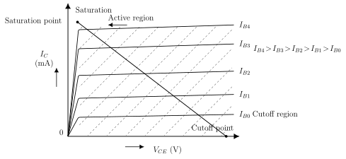
The DC load line is a straight line drawn on the transistor's output characteristics that represents every possible pair of output DC voltage and output direct current under no-signal conditions. For any given circuit the maximum output current (the saturation current) and the maximum output voltage (the cutoff voltage) are fixed by the circuit elements; these two extremes are plotted on the vertical axis and the horizontal axis respectively (figure 2.1.1). Because the values are fixed for the applied DC source, the straight line joining them is the DC load line, and its usefulness is that it contains every operating point the circuit can take.
Finding the end points of the load line
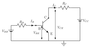
Consider a common-emitter circuit driven by two DC sources — in the base loop and in the collector loop (figure 2.1.2). Applying Kirchhoff's voltage law to the base loop gives , so the base current is
Applying KVL to the collector loop gives , which rearranges to and to
This has the form , confirming that the load line is a straight line. Its two end points are found by taking each variable to zero:
- setting gives the X-axis (cutoff) point ;
- setting gives the Y-axis (saturation) point .
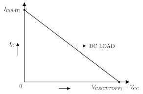
Joining these two points gives the DC load line (figure 2.1.3).
The Q point (operating point / quiescent point)
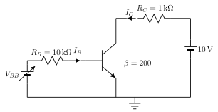
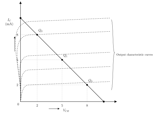
When the input signal is zero, the intersection of the load line with the transistor's output characteristic curve fixes a single point called the Q point, also known as the operating point or quiescent point. It is fixed by the applied DC voltages. Using the fixed-bias circuit of figure 2.1.7 — with , , and — the source is varied to set the base current. For the collector current is and , giving point at the middle of the load line. A larger base current (, giving , ) pushes point near saturation, while a smaller base current (, giving , ) pushes point near cutoff (figure 2.1.8). The operating point can therefore be placed anywhere along the load line depending on the application; the point carrying the zero-signal collector current and voltage has coordinates .
Selecting the operating point on the load line
Where the operating point is placed depends on the job the transistor must do:
- For switching, the operating points are chosen in the saturation region (a closed switch) and the cutoff region (an open switch).
- For amplification, the operating point is placed at the centre of the load line so that the signal is amplified faithfully.
For a transistor to work as an amplifier it must operate in the active region, which requires the emitter-base junction to be forward biased and the collector-base junction to be reverse biased. Biasing is usually done with two power supplies, but it can also be arranged with a single supply. The most commonly used biasing methods are: (i) fixed bias (base bias), (ii) collector-to-base feedback bias, (iii) emitter feedback bias, and (iv) voltage divider bias (universal bias). Of these, voltage divider bias is the most widely used.
Voltage divider bias (universal bias)
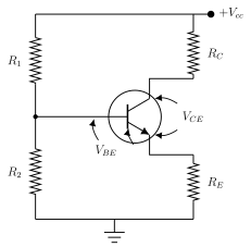
Voltage divider bias is the most widely used arrangement in the initial stages of amplifier circuits (figure 2.1.9, drawn with an npn transistor). Biasing is set by a proper choice of , and : resistors and form a potential divider across the supply , and the voltage developed across forward-biases the emitter-base junction. The emitter resistor provides stability for the operating point.
How the emitter resistor stabilises the Q point: if the collector current rises because a temperature change alters , the emitter current also rises, so the drop across increases. This larger emitter-resistor drop reduces , which in turn lowers the base current and hence brings back down — automatically opposing the original increase.
Circuit analysis: the divider voltage across is . Applying KVL to the base loop, , so ; since , . The collector loop gives . Because does not appear in these expressions, the Q point is essentially independent of , which gives excellent stabilisation. The one drawback is that also provides AC feedback, which reduces the voltage gain; this is corrected by connecting a bypass capacitor in parallel with .
End points and Q point for voltage divider bias (approximate analysis)
Starting from , the load-line end points are:
- gives the X-axis point ;
- gives the Y-axis point .
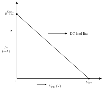
The straight line joining them is the DC load line for voltage divider bias (figure 2.1.10). For the Q point, the base loop gives , so with ,
and the collector loop gives
Together and define the operating point.
Advantages of voltage divider bias
Voltage divider bias offers three main advantages:
- The Q point does not shift, giving excellent stabilisation, because the stabilisation does not depend on .
- It is used in almost all amplifier circuits.
- It provides better amplification when used in amplifiers.
Leakage currents
Current conduction in a BJT is carried by both majority and minority charge carriers. The emitter region emits majority carriers that are collected by the collector to form the main collector current ; in addition, a small minority-carrier component flows because the collector-base junction is reverse biased — this is the collector-to-base leakage current . The total collector current is therefore
The leakage current is very small compared with the majority-carrier current. In general, the flow of current due to minority carriers under reverse-bias conditions is called the leakage current. Two leakage currents are important:
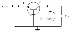
(I) Collector-to-base leakage current : with the emitter terminal open and the collector-base junction reverse biased (figure 2.1.14), the current that still flows in the collector is . It depends on temperature (thermal generation of electron-hole pairs — it roughly doubles for every 10 °C rise in a silicon transistor) and on the reverse-bias voltage.
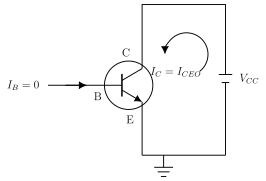
(II) Collector-to-emitter leakage current : with the base terminal open and the collector reverse biased (figure 2.1.15), the collector current is . It too depends on temperature and on the reverse voltage.
The two are related. Using , and , solving gives
Thermal runaway …
A bipolar junction transistor whose terminals are not connected to any voltage source. It carries no useful current and is never used in actual practice. Since no junction is forward or reverse biased, the device stays inactive — an external DC source is what places it in the active, saturat …
The application of a DC voltage of the correct polarity and suitable magnitude across a transistor's terminals so that it operates in the desired region for amplification, oscillation or switching. Biasing fixes the DC operating conditions — , , and — without which the tran …
A straight line on the output characteristics giving every possible pair of no-signal output voltage and output current , drawn between the fixed saturation and cutoff end points. Its usefulness is that it contains every operating point the circuit can take, since both end points a …
The point where the DC load line intersects the output characteristic curve when the signal is zero; fixed by the applied DC voltages and written . Its coordinates carry the zero-signal values and ; for faithful amplification it is placed at the centre of the …
A biasing method in which and form a potential divider across and stabilises the operating point; also called universal bias and preferred because the Q point …
The small current that flows because of minority charge carriers when a transistor junction is reverse biased. In a BJT the reverse-biased collector-base junction contributes — very small next to the majority-carrier collector current, but it roughly doubles for every 10 °C rise in a sil …
The self-destruction of a transistor caused by a cumulative rise in temperature and leakage current that drives the operating point into saturation until the junctions may burn out. The loop is cumulative: a larger heats the collector junction, raising , which raises again — which is why the bia …
The ratio of the change in collector current to the change in reverse saturation current at constant and ; a larger value indicates greater thermal instability. Written , it measures how much temperature-driven leakage shifts the collector current, so a lo …
A device (usually a shaped copper conductor) attached to a transistor to absorb the heat generated inside it and radiate it to the surroundings, raising the effective power ra …
and , from KVL on the base and collector loops of figure 2.1.2. Rearranging gives , the $ …
X-axis (cutoff), set : . Y-axis (saturation), set : . Here is the collector supply voltage (in volts) and the collector resistor; joining these two fixed extremes on the and $V …
and — the coordinates of the operating point in a fixed-bias circuit (figure 2.1.7). is the current gain and the base current set by ; e.g. with and , and $V_{ …
; since , . is the divider voltage across , the base-emitter drop and the emitter resistor; because is absent, b …
. End points: at , and at . Obtained from KVL on the collector loop, with acting as the total DC load; joining the two end points gives the DC …
and , with . Because is absent, the Q point is nearly independent of . Both come from KVL — the base loop gives , the collector loop gives — and tog …
. Using , and , the two leakage currents relate as …
at constant and ; the higher , the more thermally unstable the circuit. is the change in collector current and the change in reverse saturation current; quantifies how stron …
Drawn by us to help you understand the concept clearly, and verified to make sure it's accurate. For exams, practice from your textbook's own diagram.
Shows a family of – output curves for increasing base currents up to , with the DC load line running from the saturation point on the axis down to the cutoff point on the axis and the active region in between. Illustrates how the lo …
Drawn by us to help you understand the concept clearly, and verified to make sure it's accurate. For exams, practice from your textbook's own diagram.
An npn transistor with base source through and collector source through , marking , , and . This is the circuit whose KVL equations give th …
Drawn by us to help you understand the concept clearly, and verified to make sure it's accurate. For exams, practice from your textbook's own diagram.
A straight line, labelled DC LOAD, from on the axis to on the axis (figure 2.1.3). Notice that the line's slope is : every no-signal pair the circuit can take lies on this li …
Drawn by us to help you understand the concept clearly, and verified to make sure it's accurate. For exams, practice from your textbook's own diagram.
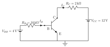
A two-source CE circuit with numeric component values (, , , ) used to work out and $I_ …
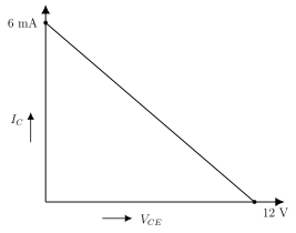
Drawn by us to help you understand the concept clearly, and verified to make sure it's accurate. For exams, practice from your textbook's own diagram.
The straight load line for figure 2.1.4, from to (figure 2.1.5). The intercepts follow from the component values: , and $V_{CE(cutoff)} = V_{CC} = 12,\text …
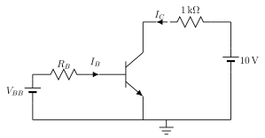
Drawn by us to help you understand the concept clearly, and verified to make sure it's accurate. For exams, practice from your textbook's own diagram.
A CE biasing circuit whose 1 kΩ collector resistor gives a saturation current of ; used to compare load-line slopes (figure 2.1.6a). Compare it with the 5 kΩ circuit of figure 2.1.6b: the smaller collector resistor gives the larger saturation current …
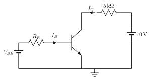
Drawn by us to help you understand the concept clearly, and verified to make sure it's accurate. For exams, practice from your textbook's own diagram.
The same form as figure 2.1.6a but with a 5 kΩ collector resistor, giving a saturation current of only (figure 2.1.6b). With the same 10 V supply, the larger lowers from 10 mA to 2 mA, so its load line is shallo …
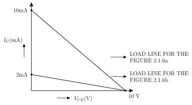
Drawn by us to help you understand the concept clearly, and verified to make sure it's accurate. For exams, practice from your textbook's own diagram.
Both load lines share the 10 V cutoff point; the 1 kΩ circuit reaches 10 mA and the 5 kΩ circuit only 2 mA on the axis (figure 2.1.6c). Notice both lines meet the voltage axis at the same cutoff point ; only the slope differs, so a larger collector re …
Drawn by us to help you understand the concept clearly, and verified to make sure it's accurate. For exams, practice from your textbook's own diagram.
Varying sets the base current so that different Q points can be calculated along the load line (figure 2.1.7). For it gives and — the mid-line point ; larger or smaller base cur …
Drawn by us to help you understand the concept clearly, and verified to make sure it's accurate. For exams, practice from your textbook's own diagram.
Q1 sits at the middle of the load line, Q2 near saturation and Q3 near cutoff, showing how the choice of base current moves the operating point (figure 2.1.8). (, ) suits faithful amplification; and show why a drifting bias risks distortion as the signal swings into saturation or cutoff. …
Drawn by us to help you understand the concept clearly, and verified to make sure it's accurate. For exams, practice from your textbook's own diagram.
and set the base voltage across while stabilises the operating point; and are marked. This is the circuit analysed for the -i …
Drawn by us to help you understand the concept clearly, and verified to make sure it's accurate. For exams, practice from your textbook's own diagram.
A straight DC load line from on the current axis to on the voltage axis (figure 2.1.10). Note that the saturation intercept uses the total DC load , not alone, so this line is shallower than a fixed-bia …
Drawn by us to help you understand the concept clearly, and verified to make sure it's accurate. For exams, practice from your textbook's own diagram.
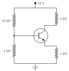
The circuit whose load-line end points and Q point are estimated in the chapter's worked problems (figure 2.1.11). Trace the divider action: sets the base voltage, fixes , and …
Drawn by us to help you understand the concept clearly, and verified to make sure it's accurate. For exams, practice from your textbook's own diagram.
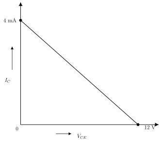
Load line for figure 2.1.11, from to (figure 2.1.12). The saturation intercept uses the total DC load: , while the cutoff intercept …
Drawn by us to help you understand the concept clearly, and verified to make sure it's accurate. For exams, practice from your textbook's own diagram.
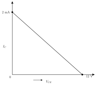
Load line for the problem with a 5 kΩ collector resistor and a 1 kΩ emitter resistor, from to (figure 2.1.13). Here the total DC load is , so ; the cutoff intercept re …
Drawn by us to help you understand the concept clearly, and verified to make sure it's accurate. For exams, practice from your textbook's own diagram.
With (emitter open), the collector still carries through the reverse-biased collector-base junction, illustrating the collector-to-base leakage current (figure 2.1.14). Note the current path from collector to base while the open emitter carries nothing; this gro …
Drawn by us to help you understand the concept clearly, and verified to make sure it's accurate. For exams, practice from your textbook's own diagram.
With (base open), the collector carries , illustrating the collector-to-emitter leakage current (figure 2.1.15). Compare with figure 2.1.14: here the leakage crosses both junctions to the emitter, and since it i …