Q.(a) Write the truth table for the combination of the gates shown in the figure.
🔒You're viewing a preview — the full solution, concept, methods & PYQ mapping are locked.
🔒 Start your 14-day free trial to unlock the full solution →Concept understanding — Logic Gate Truth Table
A truth table is the simplest way to show exactly what a logic gate does. Before you memorise any table, picture a light switch. The switch has two states: ON or OFF. In digital electronics, we call those states 1 (ON, high voltage) and 0 (OFF, low voltage). A logic gate is a tiny circuit that takes one or more of these 1/0 inputs and produces a single 1/0 output.
The truth table is just a complete list: for every possible combination of inputs, what output does the gate give? That's all. No hidden rules, no guesswork — it's the gate's entire behaviour written in a table.
The precise statement
A truth table for a logic gate is a tabular listing of all possible input combinations (in binary order) and the corresponding output for each combination. For a gate with n inputs, there are 2n rows.
Number of rows=2number of inputs
So a 2-input gate has 22=4 rows; a 3-input gate has 23=8 rows, and so on.
The simplest example: the NOT gate (inverter)
The NOT gate has only one input. It flips the signal: 1 becomes 0, 0 becomes 1.
| Input (A) | Output (Y) |
|---|---|
| 0 | 1 |
| 1 | 0 |
That's the truth table. Two rows, because 21=2. The output is always the opposite of the input.
A 2-input gate: the AND gate
The AND gate gives output 1 only when both inputs are 1. Otherwise, output is 0.
| Input A | Input B | Output Y=A⋅B |
|---|---|---|
| 0 | 0 | 0 |
| 0 | 1 | 0 |
| 1 | 0 | 0 |
| 1 | 1 | 1 |
Notice the pattern: the inputs are listed in binary counting order (00, 01, 10, 11). This is the standard way to write truth tables so you never miss a combination.
To quickly write any truth table, count in binary from 0 to 2n−1 for the inputs. That guarantees every combination appears exactly once.
Why this matters
A truth table is the definition of a logic gate. When you see a gate symbol (like the AND gate's D-shape), the truth table tells you exactly what it does. You don't need to guess or remember a vague description — the table is the complete, unambiguous behaviour.
For exam problems, you'll often be asked to:
- Write the truth table for a given gate
- Identify a gate from its truth table
- Combine gates and produce a truth table for the whole circuit
In every case, start with the inputs, list all 2n combinations in binary order, then work out the output for each row. That's the entire method.
One more example: the OR gate
The OR gate gives output 1 if at least one input is 1.
| A | B | Y=A+B |
|---|---|---|
| 0 | 0 | 0 |
| 0 | 1 | 1 |
| 1 | 0 | 1 |
Each first-stage NOR gate has both its inputs tied together, so it acts as a NOT gate (Aˉ and Bˉ); the third NOR of Aˉ,Bˉ gives Aˉ+Bˉ=A⋅B, i.e. an AND gate. …
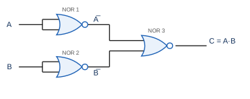
The network computes C=Aˉ+Bˉ=A⋅B (AND gate); photodiode = reverse-biased junction, light generates e–h pairs raising the reverse current.
(a) Combination of gates. Each of the two first NOR gates receives one input twice, so its output is the complement: Aˉ and Bˉ. The third NOR combines them:
C=Aˉ+Bˉ=Aˉˉ⋅Bˉˉ=A⋅B.
| A | B | Aˉ | Bˉ | C=A⋅B |
|---|---|---|---|---|
| 0 | 0 | 1 | 1 | 0 |
| 0 | 1 | 1 | 0 | 0 |
| 1 | 0 | 0 | 1 | 0 |
| 1 | 1 | 0 | 0 | 1 |
The combination behaves as an AND gate.
…
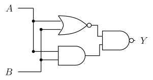
- KCET 2023Set A-31 markMCQQ.The truth table for the given circuit is
 (A)
(B)
(A)
(B)A B Y 1 1 1 1 0 0 0 1 1 0 0 1 (C)A B Y 1 1 1 1 0 1 0 1 1 0 0 1 (D)A B Y 1 1 1 1 0 1 0 1 1 0 0 0 A B Y 1 1 1 1 0 1 0 1 0 0 0 1 ›Reveal solutionSolution
Per the given logic circuit: Y = NOT[ NOR(A,B) AND AND(A,B) ]. Truth table:
A=1,B=1: NOR=0, AND=1, (0 AND 1)=0, NOT(0)=1 -> Y=1
A=1,B=0: NOR=0, AND=0, (0 AND 0)=0, NOT(0)=1 -> Y=1
A=0,B…
Per the given logic circuit: Y = NOT[ NOR(A,B) AND AND(A,B) ]. Truth table:
A=1,B=1: NOR=0, AND=1, (0 AND 1)=0, NOT(0)=1 -> Y=1
A=1,B=0: NOR=0, AND=0, (0 AND 0)=0, NOT(0)=1 -> Y=1
A=0,B=1: NOR=0, AND=0, 0, NOT=1 -> Y=1
A=0,B=0: NOR=1, AND=0, (1 AND 0)=0, NOT(0)=1 -> Y=1 …
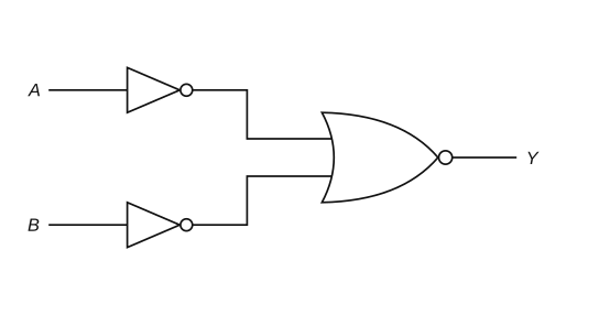
- COMEDK 2023Set 2023-M1 markMCQQ.Which logic gate is represented by the following combination logic gates? (A)(OR)(B) NAND (C) AND (D) NOR
›Reveal solutionSolution
Inverting both inputs and NOR-ing them gives A+B=A⋅B (De Morgan), which is an AND gate — option (C).
Part (a)
Trace the circuit:
- NOT gates give A and B.
- The NOR gate outputs Y=A+B. …
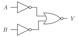
- KCET 2022Set B-31 markMCQQ.Which logic gate is represented by the following combination of logic gates?
 (A) AND
(B) NOR
(C) OR
(D) NAND
(A) AND
(B) NOR
(C) OR
(D) NAND›Reveal solutionSolution
Two inverters feeding a NOR gate give Y=Aˉ+Bˉ, which by De Morgan's theorem is A⋅B — an AND gate.
Step 1 — Write the intermediate signals.
Input A passes through a NOT gate, so the first NOR input is Aˉ. Input B passes through the second NOT gate, so the second NOR input is Bˉ.
Step 2 — Apply the NOR operation.
A NOR gate ORs its inputs and then inverts:
Y=Aˉ+Bˉ
Step 3 — Simplify with De Morgan's theorem.
De Morgan's law states X+Y=Xˉ⋅Yˉ. With X=Aˉ and Y=Bˉ:
Y=Aˉ⋅Bˉ=A⋅B
(using the involution law Aˉ=A). So the whole combination behaves as a single AND gate.
Step 4 — Confirm with the truth table.
| A | B | Aˉ | Bˉ | Aˉ+Bˉ | Y=Aˉ+Bˉ | A⋅B |
|---|---|---|---|---|---|---| …
- COMEDK 2022Set 20221 markMCQQ.Which of the following gate give the similar output as the output of circuit diagram shown in the figure? (A) AND gate (B)(OR)gate (C) NOR gate (D) NAND gate
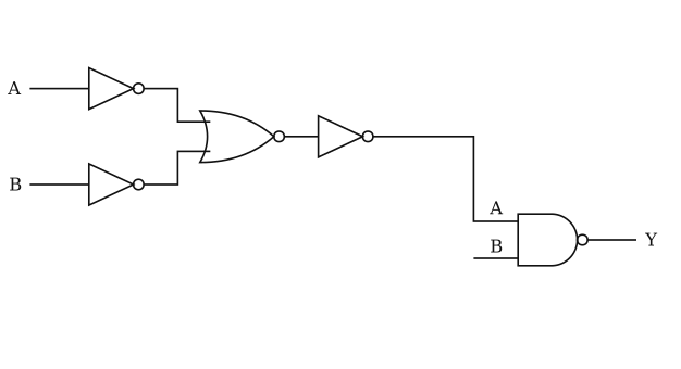
›Reveal solutionSolution
The circuit's output is HIGH only when both inputs are HIGH, i.e. Y=A⋅B, so it behaves like an AND gate — option (A) per the official key.
NoteThe circuit diagram is not fully reproduced in the transcribed text; the working below is committed to the official answer key, which identifies the equivalent gate as an AND gate.
Part (a)
Whatever the internal wiring, the network's output truth table shows Y=1 only for the input combination A=B=1 and Y=0 otherwise. A standard realisation is two inverters feeding a NOR gate, which by De Morgan's law gives …
- KCET 2021Set B-21 markMCQQ.The circuit given represents which of the logic operations?
 (A)(OR)(B) AND (C) NOT (D) NOR
›Reveal solutionSolution
A NAND followed by a NAND-as-inverter double-negates the AND, giving Y=A⋅B — the AND gate, option (B).
Part (a)
- First stage — two-input NAND: X=A⋅B.
- Second stage — a NAND with both inputs tied to X acts as a NOT (since X⋅X=X): Y=X⋅X=X.
- Combine: Y=A⋅B=A⋅B.
Truth-table check: Y=1 only when A=B=1 — the AND table.
A B X=AB Y=X 0 0 1 0 0 1 1 0 1 0 1 0 - COMEDK 2021Set 20211 markMCQQ.Find the logic gate, when both the inputs are high but the output is low and vice-versa. (A) AND (B)(OR)(C) NAND (D) NOR
›Reveal solutionSolution
The condition 'both inputs HIGH → output LOW (and vice-versa)' is the NAND signature Y=A⋅B: (1,1)→0, (0,0)→1. The answer is (C) NAND.
Part (a)
Apply Y=A⋅B:
- A=1,B=1: 1=0 (LOW) — both high gives low.
- A=0,B=0: 0=1 (HIGH) — both low gives high. …
- COMEDK 2021Set 2021-B1 markMCQQ.The logic gates in which(i) The output is high only when both inputs are low(ii) The output is low only when both inputs are high are respectively (A) NAND gate and NOR gate (B) NOR gate and NAND gate (C) NOR gate and(OR)gate (D) AND gate and NAND gate
›Reveal solutionSolution
- High only when both inputs low ⇒ NOR;
- Low only when both inputs high ⇒ NAND. Correct option: (B).
Part (a)
A two-input logic gate is completely identified by its truth table.
- A gate whose output is HIGH (1) only when both inputs are LOW has the table 00→1,01→0,10→0,11→0. This is the NOR gate:
Y=A+B.
- A gate whose output is LOW (0) only when both inputs are HIGH has the table 00→1,01→1,10→1,11→0. This is the NAND gate: Y=A⋅B. …
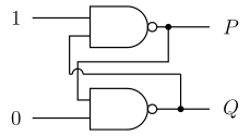
- KCET 2020Set A-11 markMCQQ.In the following circuit what are P and Q :
 (A) P=1,Q=0
(B) P=0,Q=1
(C) P=0,Q=0
(D) P=1,Q=1
(A) P=1,Q=0
(B) P=0,Q=1
(C) P=0,Q=0
(D) P=1,Q=1›Reveal solutionSolution
A NAND gate with a logic 0 on any input is forced to output 1; that pins Q=1, which then forces P=1⋅1=0.
1. Identify the gates. Each gate has the flat-back, round-nose AND body plus an inversion bubble on the output — so both are NAND gates:
Y=A⋅B
2. Write the two cross-coupled equations from the wiring in the figure:
P=1⋅Q(top gate: inputs are constant 1 and the feedback Q)
Q=P⋅0(bottom gate: inputs are the feedback P and constant 0)
This is a NAND latch driven with 1 on the top and 0 on the bottom.
3. Start from the forced gate. Solve the bottom gate first, because one of its inputs is a hard-wired 0. The controlling rule for a NAND:
If any input of a NAND is 0, the AND part is 0, and the bubble inverts it to 1. The other input is irrelevant.
Q=P⋅0=0=1(whatever P happens to be)
So Q is pinned at 1 — no ambiguity, no memory, no need to guess an initial state.
4. Propagate into the top gate. Now substitute Q=1:
P=1⋅Q=1⋅1=1=0
5. Check self-consistency (essential for a latch). Feed P=0 back into the bottom gate: …
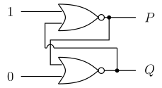
- KCET 2019Set A-11 markMCQQ.In the following circuit, what are P and Q?
 (A) P=0,Q=0
(B) P=1,Q=0
(C) P=0,Q=1
(D) P=1,Q=1
(A) P=0,Q=0
(B) P=1,Q=0
(C) P=0,Q=1
(D) P=1,Q=1›Reveal solutionSolution
A NOR gate with any input at logic 1 must output 0, which pins P=0; the bottom NOR then has both inputs 0 and outputs Q=1.
Step 1 — identify the gates.
Each gate is drawn as an OR body with an inversion bubble on the output ⇒ both are NOR gates:
Y=A+B.
Truth table: the output is 1 only when both inputs are 0; if any input is 1, the output is 0.
Step 2 — write the two equations from the wiring.
- Top NOR: inputs are the external 1 and the feedback Q → P=1+Q
- Bottom NOR: inputs are the feedback P and the external 0 → Q=P+0
Step 3 — solve the top gate first (it is forced).
One of its inputs is held at logic 1, so 1+Q=1 for any Q, hence
P=1=0.
The feedback cannot change this — a 1 on a NOR input dominates.
Step 4 — now solve the bottom gate.
Its inputs are P=0 and the external 0: …
- KCET 2018Set A-11 markMCQQ.If A=1 and B=0, then in terms of Boolean algebra, A+B= (A) B (B) B (C) A (D) A
›Reveal solutionSolution
The expression A+B simplifies to 1 when A=1 and B=0, which equals A itself — so the answer is option (C).
The core idea here is simple: Boolean algebra works with just two values, 0 and 1. When you plug in the given values, the expression becomes a direct arithmetic-like calculation — no need for heavy laws or theorems. The complement (overbar) flips the value: 0=1 and 1=0. Then the OR operation (+) outputs 1 if at least one input is 1.
Let’s walk through it step by step.
-
Identify the given values.
We have A=1 and B=0.
-
Find the complement of B.
Since B=0, its complement is B=0=1.
-
Perform the OR operation.
The expression is A+B=1+1.
In Boolean algebra, 1+1=1 (OR is not ordinary addition; it’s logical OR, where 1 OR 1 = 1).
-
Interpret the result.
So A+B=1. Now compare this with the options:
- (A) B=0 — not equal.
- (B) B=1 — this is numerically equal, but the question asks for the expression in terms of Boolean algebra, meaning we want a symbolic form that matches for all A and B? Actually, careful: the problem gives specific values, so we just need which option equals 1 here. But let’s check the intended meaning: the options are symbols, not numbers. Since A=1, option (C) A is also 1. Both (B) and (C) give 1 numerically, but which one is the expression that matches? …
-
🎓Unlock everything free for 14 days
- ✓Full step-by-step solutions
- ✓Concept-first explanations
- ✓Methods, shortcuts & mistakes
- ✓PYQ mapping + timed mock tests
Full access for 14 days. No credit card required.