Physics · Ch 14 — Semiconductor Electronics: Materials, Devices and Simple Circuits
p-n Junction Formation
p-n Junction Formation
The Starting Point: A Single Wafer
A p-n junction is not made by gluing two separate pieces of semiconductor together. Instead, we begin with a thin wafer of p-type silicon (p-Si). By carefully adding a precise amount of a pentavalent impurity (like phosphorus or arsenic) to a specific region of this wafer, that part is converted into n-type silicon. The wafer now contains a p-region, an n-region, and a boundary between them called the metallurgical junction.
A common misconception is that you can simply press a p-type slab against an n-type slab. This is impossible because even the flattest surfaces have microscopic roughness far larger than the inter-atomic spacing (~2–3 Å). Such a physical join would create a discontinuity, not a functioning junction. The junction must be formed within a single crystal.
The Two Opposing Processes: Diffusion and Drift
The formation of the junction is governed by two competing processes: diffusion and drift.
1. Diffusion Current (The Initial Driver)
In an n-type semiconductor, the concentration of electrons is much higher than the concentration of holes. In a p-type semiconductor, the opposite is true — holes are the majority carriers. At the instant the p-region and n-region are formed within the same crystal, there exists a steep concentration gradient across the junction.
- Holes diffuse from the p-side (high concentration) to the n-side (low concentration).
- Electrons diffuse from the n-side (high concentration) to the p-side (low concentration).
This directed motion of charge carriers due to a concentration gradient constitutes the diffusion current.
2. The Birth of the Depletion Region
As an electron diffuses from the n-side to the p-side, it leaves behind its parent donor atom. This donor atom, having lost an electron, becomes a positively charged ion. Crucially, this ion is immobile — it is fixed in the crystal lattice. Similarly, when a hole diffuses from the p-side to the n-side, it leaves behind an ionised acceptor atom, which is a negatively charged immobile ion.
As diffusion continues, a layer of fixed positive charge builds up on the n-side of the junction, and a layer of fixed negative charge builds up on the p-side. This region, on either side of the metallurgical junction, is called the depletion region (or space-charge region). It is called "depletion" because the mobile charge carriers (free electrons and holes) have been depleted from this area, leaving behind only the immobile ions.
The thickness of the depletion region is extremely small, on the order of one-tenth of a micrometre ().
3. Drift Current (The Opposing Force)
The fixed positive charges on the n-side and fixed negative charges on the p-side create an electric field across the junction. This field is directed from the positive charge (n-side) towards the negative charge (p-side).
This electric field exerts a force on any mobile charge carrier that enters the depletion region:
- An electron on the p-side (a minority carrier) is swept by the field towards the n-side.
- A hole on the n-side (a minority carrier) is swept by the field towards the p-side.
This motion of charge carriers due to an electric field is called drift. The resulting current is the drift current, and its direction is opposite to that of the diffusion current.
Reaching Equilibrium: The Barrier Potential
Initially, the diffusion current is very large and the drift current is very small. As diffusion continues, the depletion region widens, the electric field strengthens, and the drift current increases. This process is self-limiting. It continues until the drift current exactly balances the diffusion current. …
Drawn by us to help you understand the concept clearly, and verified to make sure it's accurate. For exams, practice from your NCERT textbook's own diagram.
What Fig. 14.10 Shows
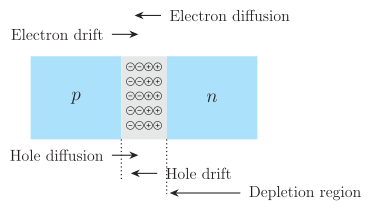
The figure is a schematic cross-section of a p-n junction during its formation. A horizontal rectangular bar is divided into two halves: the left half is labelled p (p-type semiconductor) and the right half is labelled n (n-type semiconductor). The vertical line where they meet is the metallurgical junction.
Straddling this junction is the depletion region — a narrow zone, roughly one-tenth of a micrometre wide, that contains no free charge carriers. On the p-side of this region, you see a row of minus signs: these represent immobile negative ionised acceptor cores (the fixed atoms that have accepted an electron). On the n-side, a row of plus signs represents immobile positive ionised donor cores (the fixed atoms that have donated an electron). These fixed charges do not move — they are locked into the crystal lattice.
An arrow labelled E points from the n-side (positive) toward the p-side (negative), showing the direction of the electric field that develops across the depletion region.
Two sets of current arrows appear, moving in opposite directions. One set shows diffusion current: holes moving from p to n, and electrons moving from n to p — both driven by the concentration gradient. The other set shows drift current: holes moving from n to p, and electrons moving from p to n — both driven by the electric field.
The Physical Idea
The figure teaches the central concept of dynamic equilibrium in a p-n junction. When the two regions are first brought together, there is a huge concentration difference: holes are abundant in p, electrons are abundant in n. This gradient drives diffusion — holes cross into n, electrons cross into p.
But every time a hole leaves the p-side, it leaves behind a fixed negative acceptor ion. Every time an electron leaves the n-side, it leaves behind a fixed positive donor ion. These immobile charges build up on either side of the junction, creating an electric field that points from the positive n-side toward the negative p-side. …
Drawn by us to help you understand the concept clearly, and verified to make sure it's accurate. For exams, practice from your NCERT textbook's own diagram.
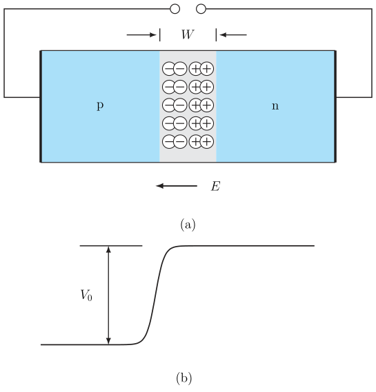
Figure 14.11 is the first picture of a p-n junction in its equilibrium state — the state where no battery is connected and no current flows. It has two panels, (a) and (b), and together they tell you what the junction looks like physically and what the electrical condition is across it.
Panel (a) shows a cross-section of the junction. On the left is the p-side, on the right is the n-side. Right at the meeting line — the metallurgical junction — you see a region that is empty of free charge carriers: the depletion region. Inside that region, the only charges left are the immobile ion cores. On the p-side of the depletion region, those are negatively charged acceptor ions (the fixed signs). On the n-side, they are positively charged donor ions (the fixed signs). Outside the depletion region, the material is neutral — the free electrons and holes still exist there, but they are not drawn. The label “V = 0” tells you that no external voltage is applied; this is the equilibrium condition.
Panel (b) is a graph. The horizontal axis is position along the junction — from the p-side on the left to the n-side on the right. The vertical axis is electric potential. The curve is a smooth rising step: it starts at a low potential on the p-side, climbs steadily across the depletion region, and levels off at a higher potential on the n-side. The total height of this step is labelled , the barrier potential. This is the built-in voltage that exists across the junction even when no battery is connected.
The barrier potential is the reason no net current flows at equilibrium. It opposes the diffusion of majority carriers — holes trying to go from p to n, and electrons trying to go from n to p — and exactly balances the diffusion current with an equal and opposite drift current.
The physical idea is this: when the p and n regions are first brought together, diffusion of carriers creates the depletion region and the electric field. That field produces the potential difference . Once is established, the drift current it drives cancels the diffusion current exactly. The junction is in equilibrium — no net current, but a permanent internal voltage exists. …