Physics · Ch 14 — Semiconductor Electronics: Materials, Devices and Simple Circuits
p-n Junction Diode under Reverse Bias
p-n Junction Diode under Reverse Bias
Reverse Bias: The Blocking State
When the external voltage is connected so that the n-side is positive and the p-side is negative, the diode is said to be in reverse bias. This is the opposite of forward bias, and the diode's behaviour changes dramatically.
The applied voltage now acts in the same direction as the built-in barrier potential . Instead of reducing the barrier, it adds to it. The effective barrier height becomes:
where is the magnitude of the applied reverse voltage. This increased barrier is the fundamental reason for the diode's behaviour under reverse bias.
A common confusion: In reverse bias, the applied voltage does not "push" carriers across the junction. It pulls them away from it. The positive terminal attracts electrons from the n-side, and the negative terminal attracts holes from the p-side, widening the depletion region.
Effect on the Depletion Region
The increased barrier height has two immediate physical consequences:
- The depletion region widens. The electric field across the junction becomes stronger, pulling more mobile charge carriers away from the junction and leaving behind a larger region of immobile ions.
- Diffusion current is suppressed almost completely. The large barrier () prevents the majority carriers (electrons from n-side, holes from p-side) from crossing the junction. The flow of electrons from n → p and holes from p → n becomes negligible.
The Origin of Reverse Current: Drift of Minority Carriers
If diffusion is blocked, why is there any current at all? The answer lies in the minority carriers.
On the p-side, there are a few thermally generated electrons (minority carriers). On the n-side, there are a few thermally generated holes (minority carriers). These minority carriers are in constant random motion. When they wander close to the junction, the strong electric field of the depletion region sweeps them across to the other side.
- An electron from the p-side is swept into the n-side.
- A hole from the n-side is swept into the p-side.
This movement of carriers from their minority side to their majority side constitutes the drift current.
The drift current exists under forward bias too, but it is completely swamped by the much larger diffusion current (which is in the milliampere range). Under reverse bias, the diffusion current is gone, so the tiny drift current becomes the only current we measure.
Characteristics of the Reverse Current
The reverse current has several unique properties that are crucial for understanding diode behaviour.
Property 1: The reverse current is very small. The drift current is typically in the range of a few microamperes (A). This is because the concentration of minority carriers is very low — it depends only on the thermal generation rate within the semiconductor.
Property 2: The reverse current is essentially independent of the applied voltage (up to a point). Even a small reverse voltage (a few volts) is sufficient to create an electric field strong enough to sweep all the minority carriers that reach the junction. Once this happens, increasing the voltage further does not increase the current. The current is limited by the rate at which minority carriers are generated, not by the voltage.
The reverse current is voltage-independent because it is limited by the supply of minority carriers, not by the applied electric field. This constant current is called the reverse saturation current.
Property 3: The reverse current is temperature-dependent. Since minority carriers are generated thermally, the reverse saturation current increases significantly with temperature. This is a critical consideration in circuit design.
The Breakdown Region
The voltage independence of the reverse current holds only up to a critical value called the breakdown voltage, denoted .
When , a dramatic change occurs. The reverse current increases sharply and almost vertically. Even a tiny increase in voltage beyond causes a huge increase in current.
If the reverse current is not limited by an external resistor to a value below the manufacturer's rated maximum, the diode will be destroyed by overheating. This destruction can also happen in forward bias if the forward current exceeds its rated value.
The mechanisms of breakdown (Zener breakdown and Avalanche breakdown) are discussed in a later section (14.8). For now, the key point is that general-purpose diodes are never operated in the breakdown region.
The V-I Characteristic Curve
The complete behaviour of a diode is captured in its V-I characteristic curve, obtained from the experimental setup shown in the textbook.
In the experimental circuit, a potentiometer (or rheostat) is used to vary the voltage applied to the diode smoothly. A milliammeter is used in forward bias (current is in mA), and a microammeter is used in reverse bias (current is in A).
The key features of the curve for reverse bias are:
- Very small, nearly constant current for all voltages from 0 up to .
- A sharp "knee" at , where the current suddenly shoots up.
- The current in this flat region is called the reverse saturation current.
Dynamic Resistance
For a diode, the simple static resistance () is not very useful because the V-I curve is non-linear. Instead, we define the dynamic resistance (or AC resistance) as the ratio of a small change in voltage to the corresponding small change in current:
This quantity tells us the resistance the diode offers to a small, varying signal at a particular operating point.
Dynamic Resistance
Worked Example: Calculating Diode Resistance
The textbook provides Example 14.4, which demonstrates how to calculate both forward and reverse resistance from a V-I characteristic curve.
Example 14.4: The V-I characteristic of a silicon diode is given. Calculate the resistance of the diode at (a) mA and (b) V.
Solution:
(a) Forward Bias Resistance ( mA) …
Drawn by us to help you understand the concept clearly, and verified to make sure it's accurate. For exams, practice from your textbook's own diagram.
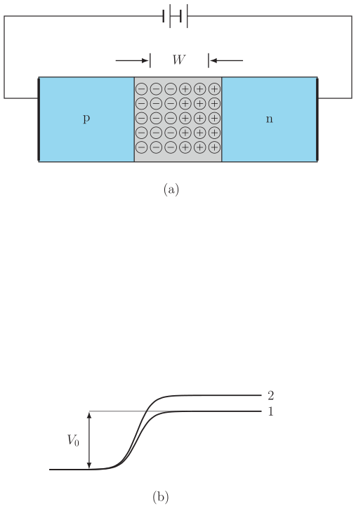
What Fig. 14.15 Shows
The figure has two panels that work together to explain what happens inside a p-n junction diode when you connect it in reverse bias.
Panel (a) shows the circuit arrangement. A battery is connected so that its positive terminal goes to the n-side of the diode and its negative terminal to the p-side. This is the defining feature of reverse bias — the polarity is opposite to what would make current flow easily. The depletion region at the junction is drawn noticeably wider than in the unbiased or forward-bias cases. The applied voltage is labelled, and the p and n sides are marked.
Panel (b) is a graph of electric potential (vertical axis) versus position (horizontal axis) across the diode. The potential rises sharply at the junction, from the p-side (low potential) to the n-side (high potential). The key point: the barrier height is now , where is the built-in potential (the barrier when no external voltage is applied) and is the applied reverse bias voltage. The step is taller than the unbiased barrier, and the region over which the potential changes is wider — matching the widened depletion region in panel (a). The labels show "p", "n", and the increased barrier .
The Physics Behind the Figure
The textbook explains that under reverse bias, the applied voltage drops almost entirely across the depletion region. Because the battery's polarity adds to the existing barrier potential (both push electrons from n to p and holes from p to n in the same direction), the net barrier becomes . This larger barrier suppresses the diffusion current — the flow of majority carriers across the junction — almost completely.
What remains is a very small current called the reverse saturation current. This current comes from minority carriers (electrons on the p-side and holes on the n-side) that randomly drift into the depletion region and get swept across by the electric field. The field direction at the junction is such that it pushes these minority carriers to their majority side, producing a tiny drift current. This current is typically in the microampere range and, importantly, does not depend much on the applied voltage — even a small reverse bias is enough to sweep all available minority carriers across.
A common mistake is to think reverse bias completely stops all current. It does not — a very small current (reverse saturation current) always flows due to minority carriers. The diode is not an ideal one-way switch; it has a small leakage current in reverse bias.
The Key Formula
The central result from this figure is the expression for the effective barrier height under reverse bias:
Where:
- is the built-in potential (also called barrier potential) of the unbiased junction — typically about 0.7 V for silicon and 0.3 V for germanium.
- is the magnitude of the externally applied reverse bias voltage (taken as positive in this expression). …
Drawn by us to help you understand the concept clearly, and verified to make sure it's accurate. For exams, practice from your textbook's own diagram.
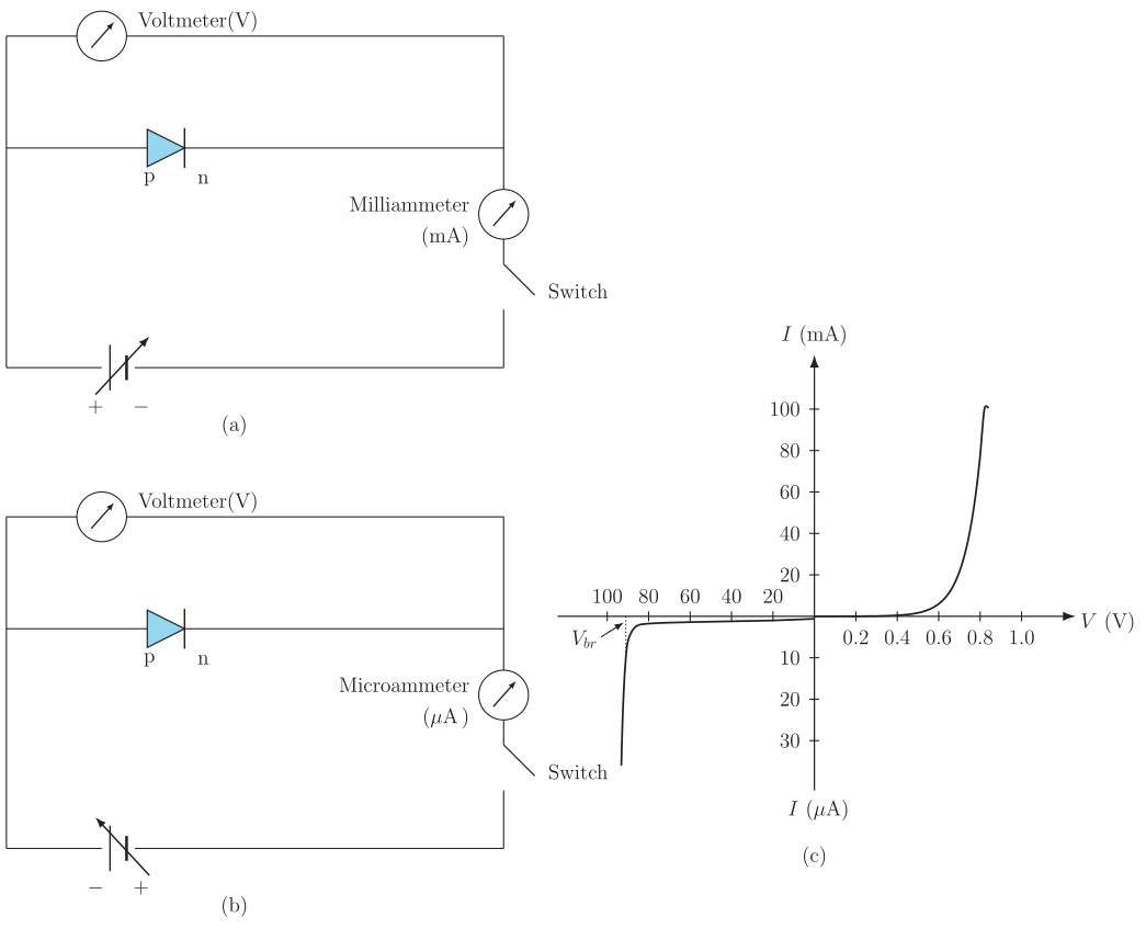
Fig. 14.16 is the central experimental reference for the entire diode section. It shows you exactly how to set up the measurement and what the result looks like. The figure has three panels, and each one teaches a distinct idea.
Panel (a) — forward bias circuit. The p-side of the diode is connected to the positive terminal of the battery, the n-side to the negative. A milliammeter (mA) is placed in series to measure the forward current, which can be tens of milliamperes. A voltmeter (V) is connected directly across the diode to read the voltage drop. A potentiometer (or rheostat) in the circuit lets you vary the applied voltage smoothly from zero upward. The key point: in forward bias, the external voltage opposes the built-in barrier, so once the applied voltage exceeds the threshold, current flows easily.
Panel (b) — reverse bias circuit. The battery is reversed: n-side to positive, p-side to negative. The series ammeter is now a microammeter (µA) because the reverse current is tiny — typically a few microamperes. The voltmeter still sits across the diode. The potentiometer again allows you to vary the voltage, but now you are increasing the reverse bias. The physical idea: the external voltage adds to the barrier, so almost no majority carriers cross; only the minority carriers that drift across produce a very small, nearly constant current.
Panel (c) — the V-I characteristic curve. This is the payoff. The horizontal axis is voltage : forward bias to the right (positive), reverse bias to the left (negative). The vertical axis is current : positive upward for forward current, negative downward for reverse current.
The forward branch starts at the origin. For small forward voltages (below about 0.7 V for silicon), the current is negligible — the diode is still "off." Then at the threshold voltage (also called cut-in voltage, for Si), the current rises steeply and almost linearly with voltage. This is the "on" region.
The reverse branch is almost flat along the negative voltage axis: a tiny, constant current called the reverse saturation current (typically a few µA). This current is independent of voltage because it is limited only by the number of minority carriers available. At a large negative voltage called the breakdown voltage , the current suddenly shoots downward (increases in magnitude sharply). If not limited by an external resistor, this can destroy the diode.
A common mistake is to think the reverse current is zero. It is not — it is just very small (µA). Also, the forward current does not become large instantly at zero voltage; there is a clear "dead zone" below the threshold.
The textbook uses this figure to define the dynamic resistance of a diode:
where is a small change in voltage across the diode and is the corresponding small change in current. For forward bias, is small (of order 10 ). For reverse bias, is huge (of order ). This enormous difference in resistance — low in forward bias, high in reverse bias — is the physical basis of rectification. …