Physics · Ch 15 — Semiconductor Electronics: Materials, Devices and Simple Circuits
Extrinsic Semiconductor
Extrinsic Semiconductor
Extrinsic Semiconductors
Pure intrinsic semiconductors — silicon and germanium — have very low conductivity at room temperature. Their conductivity does increase with temperature, but even at typical operating temperatures it remains far too low to build useful electronic devices. The solution is to deliberately introduce a small amount of a suitable impurity into the pure crystal. This process is called doping, the impurity atoms are called dopants, and the resulting material is an extrinsic semiconductor (also called an impurity semiconductor).
The amount of impurity added is tiny — just a few parts per million (ppm). Yet this small addition increases the conductivity by many orders of magnitude. The dopant atoms must be chosen carefully: their size must be nearly the same as the host atoms (Si or Ge) so that they fit into the crystal lattice without distorting it. They occupy only a very few of the original atom sites.
For tetravalent Si or Ge (Group 14 of the periodic table), two types of dopants are used:
- Pentavalent (valency 5): Arsenic (As), Antimony (Sb), Phosphorus (P)
- Trivalent (valency 3): Indium (In), Boron (B), Aluminium (Al)
These two classes of dopants produce two fundamentally different types of extrinsic semiconductors.
n-Type Semiconductor
When a pentavalent atom replaces a Si or Ge atom in the crystal lattice, four of its five valence electrons form covalent bonds with the four neighbouring Si atoms. The fifth electron remains very weakly bound to its parent atom. Why? Because the four bonding electrons are effectively part of the atom's core as far as the fifth electron is concerned — it sees a net positive charge of only +1e, not +5e. The ionisation energy required to set this fifth electron free is therefore very small:
- For germanium: about 0.01 eV
- For silicon: about 0.05 eV
Compare this with the energy required to jump the forbidden band in the intrinsic semiconductor: about 0.72 eV for Ge and about 1.1 eV for Si at room temperature. The extra electron is essentially free even at room temperature.
The pentavalent dopant donates one extra electron for conduction. Such impurities are called donor impurities.
The number of conduction electrons contributed by the donor atoms depends strongly on the doping level and is independent of any increase in ambient temperature. In contrast, the number of free electrons (and an equal number of holes) generated intrinsically by the Si atoms themselves increases only weakly with temperature.
In a doped semiconductor, the total number of conduction electrons comes from two sources: electrons contributed by donors and those generated intrinsically. The total number of holes comes only from the intrinsic source. However, the rate of recombination of holes increases because there are now many more electrons available. As a result, the number of holes gets reduced further.
With proper doping, the number of conduction electrons can be made much larger than the number of holes. Hence, in an extrinsic semiconductor doped with a pentavalent impurity:
- Electrons are the majority carriers
- Holes are the minority carriers
Such semiconductors are called n-type semiconductors (n for negative charge carriers).
p-Type Semiconductor
When a trivalent impurity atom (like Al, B, or In) replaces a Si or Ge atom, the situation is different. The trivalent atom has only three valence electrons — one less than the host atom. It can form covalent bonds with three neighbouring Si atoms, but it has no electron to offer to the fourth Si neighbour. The bond between the fourth neighbour and the trivalent atom therefore has a vacancy — a hole.
Now, a neighbouring Si atom in the lattice wants an electron to fill this vacancy. An electron from the outer orbit of a nearby atom may jump to fill the hole, leaving a vacancy (a hole) at its own original site. That hole is now available for conduction.
When the trivalent atom accepts the fourth electron from a neighbouring Si atom, it becomes effectively negatively charged. Such impurities are called acceptor impurities.
One acceptor atom gives one hole. These holes are in addition to the intrinsically generated holes, while the only source of conduction electrons is intrinsic generation. The recombination process reduces the number of intrinsically generated electrons down to .
For p-type semiconductors:
- Holes are the majority carriers
- Electrons are the minority carriers
The crystal as a whole maintains charge neutrality. The charge of the additional charge carriers (electrons in n-type, holes in p-type) is exactly equal and opposite to the charge of the ionised cores in the lattice. The dopant, by adding a large number of current carriers of one type, indirectly helps to reduce the intrinsic concentration of minority carriers — because the minority carriers have a much higher chance of meeting majority carriers and recombining.
Energy Band Structure of Extrinsic Semiconductors
Doping affects the energy band structure of the semiconductor. In extrinsic semiconductors, additional energy states appear within the forbidden gap due to the impurity atoms.
n-Type: Donor Energy Level
For an n-type semiconductor, the donor energy level lies slightly below the bottom of the conduction band . Electrons from this level can move into the conduction band with a very small supply of energy — much less than the band gap energy. At room temperature, most donor atoms are ionised, but only about atoms of Si per cubic metre are ionised intrinsically. So the conduction band contains mostly electrons that came from the donor impurities.
p-Type: Acceptor Energy Level
For a p-type semiconductor, the acceptor energy level lies slightly above the top of the valence band . With a very small supply of energy, an electron from the valence band can jump to the level , ionising the acceptor atom negatively. (Equivalently, we can say that a hole from level sinks down into the valence band — electrons rise up and holes fall down when they gain external energy.) At room temperature, most acceptor atoms are ionised, leaving holes in the valence band. The density of holes in the valence band is therefore predominantly due to the impurity.
The Mass Action Law
In any semiconductor in thermal equilibrium — whether intrinsic or extrinsic — the product of electron and hole concentrations is a constant that depends only on the material and temperature.
where is the intrinsic carrier concentration (the number of electrons or holes per unit volume in the pure, undoped semiconductor at the same temperature).
This relation is crucial. For an n-type semiconductor where is very large, becomes correspondingly very small — and vice versa for p-type.
Example: Calculating Carrier Concentrations
›Proof
Example 14.2 (NCERT)
Suppose a pure Si crystal has atoms m. It is doped by 1 ppm concentration of pentavalent As. Given that m, calculate the number of electrons and holes.
…
Drawn by us to help you understand the concept clearly, and verified to make sure it's accurate. For exams, practice from your textbook's own diagram.
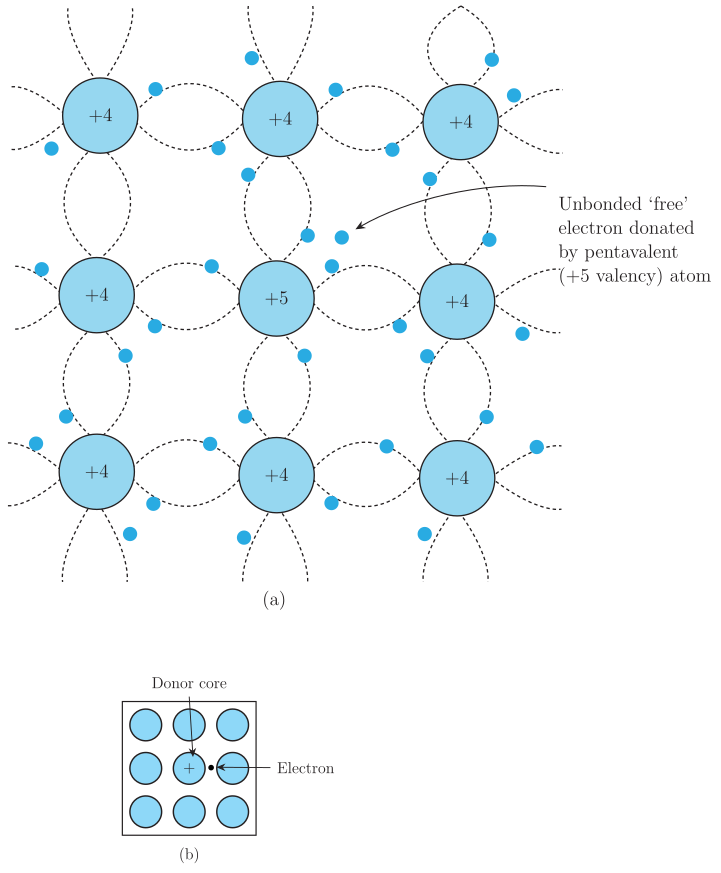
Fig. 14.7 is a two-panel illustration that shows the microscopic origin of an n-type semiconductor. The figure is not a graph with axes; it is a schematic of the crystal lattice.
Panel (a) shows a two-dimensional representation of a silicon or germanium crystal. Each host atom is drawn as a circle labelled +4, indicating its core charge (four valence electrons). One of these lattice sites is replaced by a pentavalent impurity atom — arsenic, antimony, or phosphorus — drawn as a circle labelled +5. Four of the donor’s five valence electrons form ordinary covalent bonds with the four neighbouring silicon atoms. The fifth electron is not needed for bonding; it remains loosely attached to the donor core. The figure shows this fifth electron as a separate dot near the donor, with the real printed label "Unbonded 'free' electron donated by pentavalent (+5 valency) atom". The key physical idea is that this fifth electron is bound very weakly — its ionisation energy is only about 0.05 eV in silicon and 0.01 eV in germanium — so at room temperature it is already free to move through the lattice, contributing to conduction.
Panel (b) is the simplified schematic that appears in circuit diagrams and band discussions. The donor atom is now drawn as a fixed core marked + and labelled "Donor core" (one effective positive charge, because the core has donated one electron to the lattice). Nearby, the free electron is shown as a plain filled dot (•), labelled "Electron" — not a − symbol. This schematic captures the essential physics: the donor leaves behind a stationary positive charge and supplies one mobile electron for conduction.
The central result that the textbook develops using this figure is the carrier concentration in an n-type semiconductor. Because the donor concentration (in atoms per cubic metre) is typically much larger than the intrinsic carrier concentration , the electron concentration is essentially equal to :
The hole concentration is then obtained from the law of mass action:
so that
…
Drawn by us to help you understand the concept clearly, and verified to make sure it's accurate. For exams, practice from your textbook's own diagram.
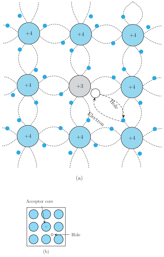
Figure 14.8 is the companion to the n-type doping diagram (Fig. 14.7) and shows how a p-type semiconductor is created at the atomic level. The figure has two panels, (a) and (b), which present the same physical situation at different levels of abstraction.
Panel (a) shows a small piece of the silicon or germanium crystal lattice drawn in two dimensions. Each host atom is represented by a core labelled +4 (the effective charge of the tetravalent Si or Ge atom after its four valence electrons are considered part of the covalent bonds). The lattice is held together by shared electron pairs — each line between two cores represents one covalent bond containing two electrons. At one lattice site, a trivalent impurity atom (labelled +3; the textbook names In, Al, or B) has replaced a host atom. Because this impurity has only three valence electrons, it can form complete covalent bonds with only three of its four silicon neighbours. The fourth bond position is empty — there is no electron pair. That empty bond is the hole, drawn as a missing bond line or a vacancy. The hole is not a particle; it is the absence of an electron where a covalent bond should be.
Panel (b) is the simplified schematic that appears in nearly every textbook and exam diagram. The entire trivalent impurity atom and its local environment are replaced by a single fixed core marked with a minus sign (−). This minus sign represents the effective negative charge that the acceptor atom acquires: once the hole is filled by an electron from a neighbouring Si atom (a process that happens almost instantly at room temperature), the acceptor atom has one extra electron permanently bound to it, giving it a net negative charge. Next to this fixed negative core is an open circle (○), labelled "Hole" — the same empty-circle convention used for holes throughout this chapter (see Fig. 14.6) — representing the hole that has now moved away into the lattice and is free to conduct, not a plus sign. The schematic thus shows the two essential features: a stationary negative ionised acceptor and a mobile positive hole.
The key physical idea is that one trivalent dopant atom creates exactly one hole available for conduction. The hole is the majority carrier in a p-type semiconductor; electrons are the minority carriers.
The textbook uses this figure to establish the carrier concentration relations for p-type material. If the acceptor concentration is (number of trivalent atoms per cubic metre), and the intrinsic carrier concentration is , then at room temperature (where nearly all acceptors are ionised) the hole concentration is approximately
because the dopant contribution completely dominates the thermally generated holes. The electron concentration is then found from the law of mass action:
Substituting gives
Since is typically to m while for Si is m, the electron concentration becomes extremely small — of order to m. This is the quantitative meaning of the statement for p-type semiconductors. …
Drawn by us to help you understand the concept clearly, and verified to make sure it's accurate. For exams, practice from your textbook's own diagram.
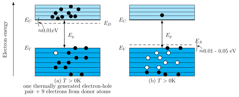
Fig. 14.9 is a pair of energy-band diagrams that show what happens inside a semiconductor after doping. The left panel (a) is for an n-type semiconductor, the right panel (b) for a p-type semiconductor. Both are drawn for a temperature above absolute zero ( K), so thermal energy is available.
In each panel, the vertical axis represents electron energy. The conduction band (labelled ) is the lowest energy an electron can have while being free to move through the crystal; the valence band (labelled ) is the highest energy an electron can have while still bound to an atom. The gap between them is the forbidden band or band gap.
Panel (a) — n-type. A short dashed line labelled appears just below , with the real figure's own printed annotation "" marking this gap. This is the donor energy level, created by pentavalent impurity atoms (like arsenic or phosphorus). Each donor atom contributes one extra electron that is very weakly bound. At room temperature, that tiny energy difference is easily supplied, so the electron leaves the donor level and moves up into the conduction band. The diagram shows filled circles (electrons) in the conduction band, representing these donated electrons that are now free to conduct. The donor level itself is drawn as a dashed line because it is not a continuous band — it is a discrete set of energy states localised at the impurity atoms.
Panel (b) — p-type. A short dashed line labelled appears just above , with the real figure's own printed annotation "" marking this gap. This is the acceptor energy level, created by trivalent impurity atoms (like boron or indium). Each acceptor atom has one fewer valence electron than the host, creating a "hole" — a missing electron. An electron from the valence band can gain a very small amount of energy and jump up into the acceptor level, filling that hole. But when the electron leaves the valence band, it leaves behind a hole there. The diagram shows empty circles (holes) in the valence band, representing these positively charged vacancies that can move and conduct current. The acceptor level is also a dashed line, for the same reason — it is a discrete set of states.
The key physical idea is that doping introduces localised energy levels inside the band gap, very close to one band edge. For n-type, the donor level is just below ; for p-type, the acceptor level is just above . This tiny energy gap (≈ 0.01-0.05 eV in Si) is what makes doping so effective — at room temperature, almost all impurity atoms are ionised, providing a huge number of majority carriers without needing the much larger band-gap energy (≈ 1.1 eV for Si).
The textbook uses this figure to develop the central relation for carrier concentrations in thermal equilibrium:
Here is the number of conduction electrons per cubic metre, is the number of holes per cubic metre, and is the intrinsic carrier concentration (the electron or hole concentration in pure, undoped silicon at the same temperature). This product is constant for a given semiconductor at a given temperature, regardless of doping.
For an n-type semiconductor, because the donor atoms supply many extra electrons. The few holes that exist come from thermal generation, but they recombine rapidly with the abundant electrons, so becomes very small. For a p-type semiconductor, the opposite holds: . …