Electronics · Ch 9 — Power Electronics and its Applications
Applications of Power Electronics
Applications of Power Electronics
Applications of Power Electronics brings the devices of the first part together into working converters. Power electronics can be described as the art of converting electrical energy from one form to another efficiently, smoothly, compactly and robustly for convenient use; the exact output — its voltage, current and frequency — depends on the load and the application.
Why power electronics keeps growing
Several practical pressures have driven the rapid growth of power electronics:
- The rising cost of electrical energy makes efficient conversion essential.
- Commercial systems such as bank computers and security installations need uninterrupted power supplies (UPS).
- Everyday equipment — lamp dimmers, water heaters, air conditioners, temperature controllers, washing machines, emergency lighting and SMPS — all use power-electronic converters.
- Industry needs variable-speed motors for precise process control.
- Electric trains and buses rely on power converters for battery charging and motor-speed control.
Power converters and the static switch
Every power semiconductor device can be used as a bistable solid-state switch with two stable states — non-conducting (OFF) and conducting (ON) — exactly like the OFF/ON states of a mechanical switch. Used this way the device is a static switch, and it has real advantages over an electromechanical switch such as a relay:
- it is completely static, with no moving parts, no arcing and silent operation;
- it is very fast, compact and long-lived;
- it is more reliable and works over a much wider range than a relay; and
- it can operate directly from the mains at high voltage and high current.
Classification of power converters
Power converters are grouped by the conversion they perform — rectifier, AC voltage controller, DC chopper and inverter — as summarised in the accompanying table.
AC to DC converter (rectifier)
Single-phase uncontrolled (diode) rectifiers are widely used to produce an intermediate, unregulated DC voltage that is then processed into regulated DC; they are efficient and robust. Their drawbacks are that they cannot control the magnitude of the output when the AC input and load are fixed, and that power flows only one way (AC to DC). Replacing the diodes with thyristors gives a controlled rectifier: because a thyristor turns on only when a gate pulse is applied and can block forward voltage until then, delaying the turn-on instant controls how much of each half-cycle reaches the load — and hence the average output voltage.
SCR half-wave rectifier with RC triggering
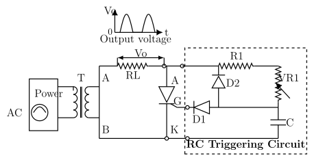
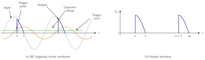
RC triggering is the most common way to control thyristor power. In the half-wave circuit (Figure 9.2.1) the SCR gate signal is taken from an RC lag network (R1, VR1, C) through diode D1, while diode D2 blocks negative gate-cathode voltage. During the positive half-cycle terminal A is positive with respect to B; the capacitor voltage lags the supply by an angle set by R1, VR1 and C. When it rises to the trigger level it supplies enough gate current to fire the SCR. The instant of firing is the firing angle ; from to the supply voltage appears across the load, giving control over the full to of the half-cycle. During the negative half-cycle the SCR cannot conduct, so the load voltage is zero. Varying VR1 changes the phase-lag angle and therefore the power delivered. Figure 9.2.2 shows the triggering waveforms and the half-wave output. The average load voltage is
and the average load current is .
For a half-wave controlled rectifier the average load voltage carries a factor of , because only one half-cycle in every full cycle reaches the load. For a full-wave controlled rectifier (below) the factor is , since both half-cycles are used. A few of the book's worked examples print the symbolic half-wave step as while working the numbers with ; the correct half-wave result is the form used above.
SCR full-wave rectifier with RC triggering
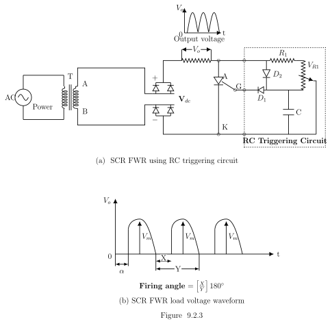
The full-wave version (Figure 9.2.3) places a single thyristor after a diode bridge. The bridge turns the AC into a unidirectional voltage, and the RC network, connected across the bridge output, produces a capacitor voltage that follows that rectified waveform. In every half-cycle, when the capacitor voltage reaches the trigger level it supplies gate current, the thyristor conducts, and voltage appears across the load. Because both half-cycles are now used, the average load voltage is
The firing angle can be read directly from the load-voltage waveform of Figure 9.2.3(b) as , where X and Y are the marked segments.
AC to AC converter (AC voltage controller)
An AC voltage controller provides a variable alternating voltage with no change in frequency, useful for domestic and industrial heating and lighting. The variable voltage is obtained with a bidirectional electronic switch — a TRIAC — connected between the AC supply and the load. By varying the RMS value of the AC delivered to the load, the power is controlled: portions of the supply sinusoid reach the load while the switch blocks the rest. A fixed-AC-to-variable-AC converter is therefore called an AC voltage controller.
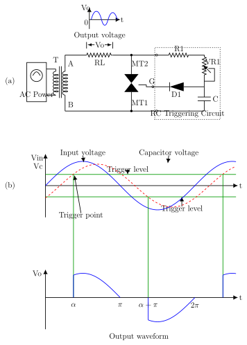
In the single-phase TRIAC controller with RC triggering (Figure 9.2.4), the TRIAC conducts in both halves of the supply. During the positive half-cycle MT2 becomes positive with respect to MT1 and the gate is made positive; injecting a gate pulse at firing angle fires the TRIAC, and load current follows the supply from to , where the device switches off by line commutation at the voltage zero-crossing. During the negative half-cycle MT2 becomes negative with respect to MT1; a gate pulse at fires the TRIAC again, and current flows from to . Adjusting each cycle sets the RMS load voltage.
DC to DC converter (DC chopper)
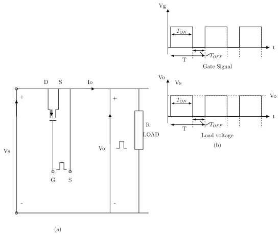
A DC chopper converts a fixed DC voltage into a variable DC output by switching the supply on and off rapidly; the output is controlled through the switch's duty cycle. It is used in variable-voltage DC supplies, battery chargers, SMPS and DC motor control. In Figure 9.2.5 a MOSFET is placed between source and load: a gate pulse switches it ON, connecting the supply to the load, and removing the gate signal switches it OFF, disconnecting the load. For a resistive load the output voltage and current follow the shape of the gate pulses. The average output voltage is
where is the ON-time and the switching period. The ratio is the duty ratio — the single most important factor governing chopper performance — and it is varied by changing the ON-period while keeping the switching frequency constant. The gate pulses are delivered through an opto-coupler isolator.
DC to AC converter (inverter)
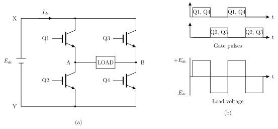
An inverter converts DC power into AC power at a desired output voltage and frequency, for uses such as variable-speed AC motor drives, aircraft power supplies and UPS systems for computers. The single-phase full-bridge inverter of Figure 9.2.6 uses four IGBTs (Q1–Q4), with only two diagonally opposite devices ON at a time. When Q1 and Q4 conduct, load current flows one way and the load voltage is ; when Q3 and Q2 conduct, the current reverses and the load voltage becomes . Alternating between these two pairs produces an AC square wave across the load. The output frequency is set by the frequency of the gate pulses, and the gate signals are injected to the IGBT gate-emitter terminals through an opto-isolator.
Gate drive circuits
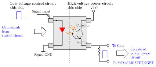
Every discrete controlled device has three terminals: two carry the main current and the third, with one main terminal, forms the control terminals. A gate drive circuit must satisfy the control-terminal requirements so as to turn each device of a converter reliably ON and OFF. Because the devices sit at different points and voltage levels in the power circuit but are commanded by one common controller, electrical isolation is essential, and each device usually needs its own isolated drive supply. There are two functional types of isolation: pulse-transformer isolation (used for thyristors — SCR and TRIAC — without a separate supply on the secondary) and optical isolation (used for MOSFETs and IGBTs, with a supply on the output side).
Pulse transformer isolator circuit
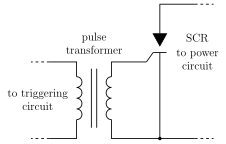
A pulse transformer provides electrical isolation between the low-voltage gate-control circuit and the high-voltage power circuit in SCR and TRIAC firing circuits — important because the power side may sit at a high AC voltage. The transformer is usually a 1:1 two-winding type with low winding and leakage resistance. In Figure 9.2.7 the gate signal from a control circuit (such as a microcontroller) is applied to the primary; the pulse it produces in the secondary is coupled to the gate and cathode of the SCR and turns it on, all without any direct electrical connection between the two sides.
Opto-coupler isolator circuit …
Drawn by us to help you understand the concept clearly, and verified to make sure it's accurate. For exams, practice from your textbook's own diagram.
Figure 9.2.1 shows the SCR half-wave rectifier: the transformer secondary (A, B), the load resistor across which the output voltage is measured, the SCR (anode A, cathode K, gate G) and the RC triggering network (R1 …
Drawn by us to help you understand the concept clearly, and verified to make sure it's accurate. For exams, practice from your textbook's own diagram.
Figure 9.2.2 shows (a) the triggering waveforms — input, lagging capacitor voltage and trigger level with the trigger point — and (b) the half-wave output, with one conduction pulse per …
Drawn by us to help you understand the concept clearly, and verified to make sure it's accurate. For exams, practice from your textbook's own diagram.
Figure 9.2.3 shows (a) the SCR full-wave rectifier — a diode bridge feeding a single thyristor with the same RC triggering network — and (b) the full-wave load-voltage waveform, from which the firing angle is read …
Drawn by us to help you understand the concept clearly, and verified to make sure it's accurate. For exams, practice from your textbook's own diagram.
Figure 9.2.4 shows (a) the single-phase TRIAC AC voltage controller (transformer, load resistor, TRIAC with MT1, MT2, gate G, and the RC trigger network) and (b) the waveforms, with conduction from to …
Drawn by us to help you understand the concept clearly, and verified to make sure it's accurate. For exams, practice from your textbook's own diagram.
Figure 9.2.5 shows (a) the chopper circuit — a MOSFET between the DC source and a resistive load — and (b) the gate-signal and load-voltage waveforms marking , and the pe …
Drawn by us to help you understand the concept clearly, and verified to make sure it's accurate. For exams, practice from your textbook's own diagram.
Figure 9.2.6 shows (a) the single-phase full-bridge inverter with four IGBTs (Q1–Q4) and the load between the bridge midpoints, and (b) the complementary gate pulses and the resulting / \ …
Drawn by us to help you understand the concept clearly, and verified to make sure it's accurate. For exams, practice from your textbook's own diagram.
Figure 9.2.7 shows a 1:1 pulse transformer coupling the gate signal from the triggering circuit to the gate and cathode of an SCR, isolating the low-voltage control side fr …
Drawn by us to help you understand the concept clearly, and verified to make sure it's accurate. For exams, practice from your textbook's own diagram.
Figure 9.2.8 shows the opto-coupler isolator: a signal from the low-voltage control side drives an infrared LED whose light switches a phototransistor on the high-voltage power side, delivering the gate drive to the MOSFET/IGBT with no direct …
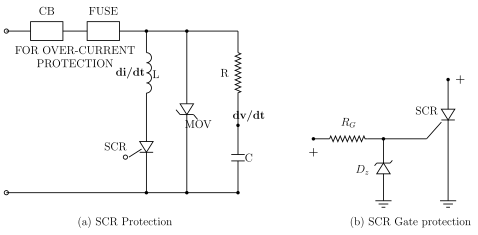
Drawn by us to help you understand the concept clearly, and verified to make sure it's accurate. For exams, practice from your textbook's own diagram.
Figure 9.2.9 shows (a) SCR protection — circuit breaker and fuse for over-current, a series inductor for , an MOV for over-voltage and an R-C snubber for — and (b) gate protection with a series gate res …
Data from the book's 'Classification of Power Converters' table (the circuit symbols are shown as figures rather than reproduced here):
| Conversion | Converter | Function |
|---|---|---|
| AC to DC | Rectifier | AC to unipolar DC current |
| AC to AC | AC voltage controller | AC of desired magnitude from the line AC |
where is the peak supply voltage and the firing angle. The factor reflects that only …
Both half-cycles are used, so the factor is — twice the half-wave …
where X and Y are the segments read from the full-wave load-voltage waveform of Figure 9.2.3(b). X is the blocked segment before the thyristor fires and Y is the length of one half-cycle, so the ratio scaled by gives the firing angle in …
The output is set by the duty ratio, varied by changing the ON-period while the period T (switc …
A power semiconductor device used in its two stable states — non-conducting (OFF) and conducting (ON) — as an electronic switch with no moving parts, no arcing and silent, fast, reliable operation, …
The instant, measured as an angle of the AC cycle, at which a thyristor or TRIAC is triggered into conduction. Delaying the firing angle reduces the portion of each half-cycle delivered to the load, which is how a controlled rectifier or …
The ratio of the ON-time to the total switching period, , of a chopper. It is the most important factor governing chopper performance and directly sets the average DC output voltage. It is varied by changing the ON-period while the switching period T (and hence frequency) …
An electronic component that transfers a signal from one circuit to another using light — an infrared LED optically in line with a phototransistor in one package — while keeping the two circuits electrically isolated. Used to drive MOSFET an …
A series R-C network connected across a power device to limit the rate of rise of voltage and absorb switching voltage spikes, protecting the device from false trig …