Electronics · Ch 9 — Power Electronics and its Applications
Power Semiconductor Devices
Power Semiconductor Devices
Power electronics begins with the switching devices themselves. This part of the chapter looks at each power semiconductor device in turn — how it is built, how it is biased, and the shape of its output characteristics. Understanding these devices is what makes the converter circuits in the second part of the chapter easy to follow.
Required properties of a power semiconductor device
A good power device must survive large voltages and carry large currents while wasting as little energy as possible. Ideally it should have:
- a large blocking (withstand) voltage in the OFF state;
- a large forward current capability and high power rating;
- a very low, ideally zero, on-state conduction drop (forward voltage drop);
- zero off-state leakage (reverse leakage) current;
- instant turn-on and turn-off; and
- the ability to withstand a large rise in temperature.
The six important power devices studied here are power diodes, power bipolar junction transistors (BJTs), silicon controlled rectifiers (SCRs), the TRIAC, power MOSFETs and IGBTs.
The power diode
A power diode is a two-terminal device that conducts a large current in the forward direction with very little power loss, while blocking a large voltage in the reverse direction. It is the simplest power switch and the building block of every rectifier.
Construction of a power diode
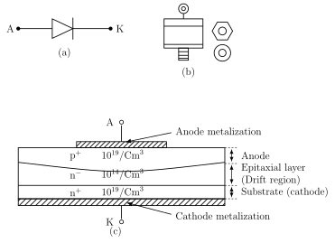
To block a large reverse voltage, a diode needs a wide depletion layer, and a wide depletion layer needs a region of low charge (low doping) density. To achieve this, a lightly doped n region — written n- and called the drift layer or epitaxial layer — is sandwiched between a heavily doped p+ anode and a heavily doped n+ cathode. The heavily doped anode and cathode have impurity densities of about , while the drift layer is lower by several orders of magnitude, about . The lightly doped drift layer gives the wide depletion region needed for reverse blocking, and its resistance is reduced during forward conduction by conductivity modulation (below). Figure 9.1.1 shows the circuit symbol, a photograph, and the layered cross-section with the anode and cathode metallisation.
Power diode under forward bias
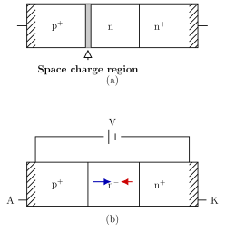
The diode is forward biased when the p+ anode is joined to the positive terminal and the n+ cathode to the negative terminal of the supply. At low forward bias, holes injected from the p+ side into the n- drift region simply recombine with electrons there. At higher forward bias (large forward current), holes from the p+ region reach the n- / n+ boundary and pull electrons out of the n+ cathode into the drift region, so that the electron density becomes equal to the hole density right across the drift region. This simultaneous injection of both carrier types is called double injection. Its consequence is conductivity modulation — the flood of extra carriers greatly increases the conductivity of the otherwise lightly doped drift layer, which is exactly what keeps the on-state voltage drop small. Figure 9.1.2 shows the junction under thermal equilibrium and under carrier injection.
Voltage drop of a forward-conducting power diode
The forward drop across a conducting power diode has two parts: the drop across the p+ n- junction and the ohmic drop across the resistive drift region. Writing for the ohmic term gives . Because the second term rises linearly with forward current, the ohmic drop makes the forward V–I characteristic of a power diode more straight-line (linear) than that of an ordinary signal diode.
Power diode under reverse bias
The diode is reverse biased when the p+ anode is joined to the negative terminal and the n+ cathode to the positive terminal. Two situations arise depending on how far the depletion layer spreads:
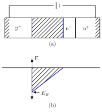
- Non-punch-through diode: the depletion boundary does not reach the end of the drift layer. The electric-field strength is maximum at the p+ n- junction and falls linearly to zero before the end of the depletion region.
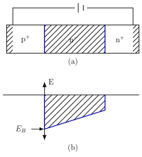
- Punch-through diode: the depletion layer spans the entire drift region and touches the n+ cathode. Because the cathode is very heavily doped, the depletion penetrates negligibly into it, so the field does not fall to zero within the drift region.
Figures 9.1.3.1 and 9.1.3.2 show the two cases together with their electric-field profiles.
V–I characteristics of a power diode
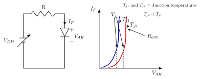
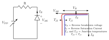
The V–I characteristics of a power diode are similar to those of a signal diode and follow the Shockley diode equation, , where is the reverse saturation current, the applied voltage, the electron charge, Boltzmann's constant and the temperature in kelvin. Both the forward and reverse characteristics depend on the junction temperature; the book plots them at two junction temperatures and (with ) in Figures 9.1.4(a) and 9.1.4(b).
Power bipolar junction transistor (PBJT)
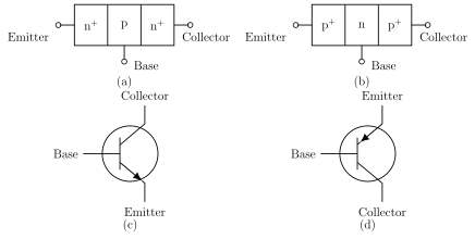
The power BJT was the first semiconductor device to give full control over both turn-on and turn-off in power circuits. It is a bipolar, current-controlled device: a small base current controls a much larger collector current. Two heavily doped n+ regions with a lightly doped p base give an npn transistor; two p+ regions with a lightly doped n base give a pnp transistor. Its three terminals are the collector, base and emitter. Figure 9.1.5 shows the npn and pnp structures and their circuit symbols.
Output V–I characteristics of a power transistor
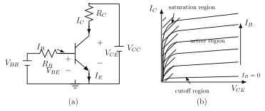
A power transistor, like a signal transistor, works in three regions, seen on the versus output characteristics (Figure 9.1.6):
- Cut-off region: with base current the collector current is almost zero.
- Active region: the base-emitter junction is forward biased and the base-collector junction reverse biased; the collector current stays fairly constant and is set mainly by the base current.
- Saturation region: as is raised, more charge is injected into the base, so base and collector currents rise; the growing drop across the external collector resistor reduces until the base-collector junction also becomes forward biased, and falls to a low value.
Silicon controlled rectifier (SCR)
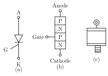
Modern power electronics truly began with the thyristor. One of the first was the four-layer p-n-p-n switch called the silicon controlled rectifier (SCR), introduced in 1958. Constructionally a thyristor is a four-layer, three-terminal controlled device. It can be turned on by a gate current pulse but cannot be turned off by the gate — the main current must be interrupted externally. It can block voltage in both directions but conducts current in only one direction. Figure 9.1.7 shows the circuit symbol, the pnpn construction (anode on the top p layer, cathode on the bottom n layer, gate connected to the lower p layer) and a photograph.
Two-transistor analogy of a thyristor
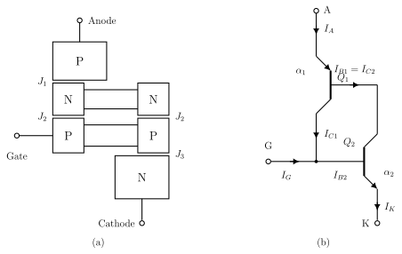
The action of the pnpn structure is best understood by splitting it into two interconnected transistors — a pnp transistor Q1 and an npn transistor Q2 — sharing the three junctions J1, J2 and J3. The collector of each transistor drives the base of the other, which is what gives the thyristor its latching behaviour. Figure 9.1.8 shows the layer division and the two-transistor equivalent circuit, with anode current , gate current , cathode current and the current gains and of Q1 and Q2.
The pnpn device under forward voltage
Consider the pnpn device with the anode positive with respect to the cathode.
(a) Gate open : junctions J1 and J3 are forward biased while J2 is reverse biased. For the two transistors, and , where and are the reverse saturation currents of the collector-base junctions. Since the anode current is , and with the gate open , substituting and solving gives
where . As long as is small, is very small and and are each well below unity, so the anode current is only slightly larger than — the device stays in its forward-blocking state.
When deriving , the textbook prints "Now from figure 9.1.10(b)". This is a cross-referencing misprint: Figure 9.1.10 is the TRIAC circuit symbol. The two-transistor equivalent circuit these equations come from is Figure 9.1.8(b), which is the reference we follow here.
(b) Gate current applied: a positive gate current lets us turn the thyristor on without raising the forward voltage all the way to its break-over level. With , the anode current becomes
A large enough drives towards unity and switches the device on for any value of . This is called gate-assisted turn-on and is the usual way a thyristor is triggered.
Static V–I characteristics of a thyristor (SCR)
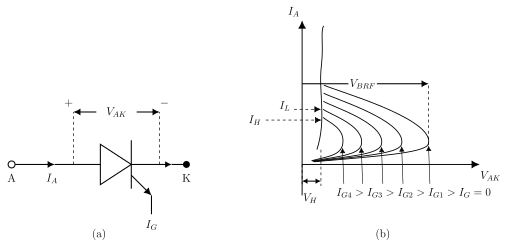
With the gate open , must rise to the forward break-over voltage before appreciable anode current flows; at that point the thyristor triggers and the voltage across it collapses to the low holding voltage (about 1–1.5 V), staying almost constant thereafter. The gate current strongly affects triggering: the larger the gate current, the lower the break-over voltage needed. Once the SCR has turned on, the gate loses control. Two currents describe the on-state:
- Latching current : the minimum anode current needed to keep the thyristor on immediately after turn-on once the gate signal is removed.
- Holding current : the minimum anode current needed to keep it on while gate current is still present.
The holding current is smaller than the latching current. Figure 9.1.9 shows the polarity diagram and the family of output characteristics for increasing gate current.
The TRIAC
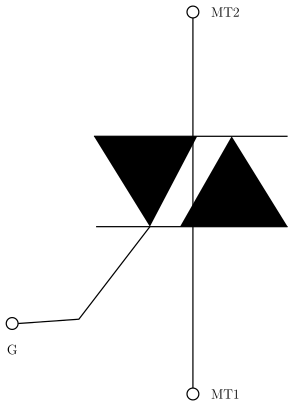
The TRIAC (Triode for AC) is a member of the thyristor family, but unlike an SCR — which conducts only from anode to cathode — a TRIAC conducts in both directions, making it a bidirectional controlled switch. This makes it ideal for AC power control, and it is widely used in residential lamp dimmers, heater control and fan-motor control. Its three terminals are Main Terminal 1 (MT1), Main Terminal 2 (MT2) and the gate G; Figure 9.1.10 shows the circuit symbol. Because either main terminal can be positive or negative and the gate can be driven either way, there are four possible triggering (electrode-potential) modes: MT2 positive with G positive, MT2 positive with G negative, MT2 negative with G negative, and MT2 negative with G positive (all referenced to MT1).
Static characteristics of a TRIAC
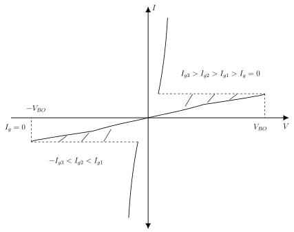
Functionally a TRIAC behaves like two thyristors connected in anti-parallel, so its V–I characteristic is symmetric: the curve in the first quadrant mirrors that in the third quadrant, each resembling the forward characteristic of a thyristor. It has a forward break-over voltage and an equal reverse break-over voltage , and increasing the gate current lowers the break-over point in either direction. With no gate signal the TRIAC blocks both half-cycles of the applied AC. Because it can be triggered at any chosen instant in each half-cycle, it gives smooth phase control of AC power. Figure 9.1.11 shows the symmetric static characteristics.
Power MOSFET …
Drawn by us to help you understand the concept clearly, and verified to make sure it's accurate. For exams, practice from your textbook's own diagram.
Figure 9.1.1 gives the three views of a power diode — the circuit symbol (anode A, cathode K), a photograph of a stud-mounted device, and the layered cross-section p+ / n- (drift/epitaxial) / n+ with doping levels of about in the p+ and n+ layers and in the drift layer. It shows why the wide, lightly doped d …
Drawn by us to help you understand the concept clearly, and verified to make sure it's accurate. For exams, practice from your textbook's own diagram.
Figure 9.1.2 shows the p+ n- n+ structure (a) at thermal equilibrium, with the space-charge region at the junction, and (b) under forward bias, where holes are injected from the p+ side and electrons from the n+ side into the drift region — the double inj …
Drawn by us to help you understand the concept clearly, and verified to make sure it's accurate. For exams, practice from your textbook's own diagram.
Figure 9.1.3.1 shows a non-punch-through diode under reverse bias, where the depletion layer does not reach the n+ cathode, together with its electric-field profile that is maximum at the p+ n- junction and falls to z …
Drawn by us to help you understand the concept clearly, and verified to make sure it's accurate. For exams, practice from your textbook's own diagram.
Figure 9.1.3.2 shows a punch-through diode, where the depletion layer spreads across the entire drift region and reaches the n+ cathode; the field profile does not fall t …
Drawn by us to help you understand the concept clearly, and verified to make sure it's accurate. For exams, practice from your textbook's own diagram.
Figure 9.1.4(a) shows the forward measuring circuit and the forward characteristic ( versus ) at two junction temperatures and (), marking the junction voltage $ …
Drawn by us to help you understand the concept clearly, and verified to make sure it's accurate. For exams, practice from your textbook's own diagram.
Figure 9.1.4(b) shows the reverse measuring circuit and the reverse characteristic: a small reverse saturation current until the reverse breakdown voltage , plott …
Drawn by us to help you understand the concept clearly, and verified to make sure it's accurate. For exams, practice from your textbook's own diagram.
Figure 9.1.5 shows the layer structures of the npn (n+ / p / n+) and pnp (p+ / n / p+) transistors and their circuit symbols, with the emitter-arrow direction distinguishing the two. The power BJT is a current-controlled device in which a small base current controls a much larger collector current; not …
Drawn by us to help you understand the concept clearly, and verified to make sure it's accurate. For exams, practice from your textbook's own diagram.
Figure 9.1.6 shows the common-emitter bias circuit (with base-emitter forward biased and base-collector reverse biased) and the family of versus output curves, marking the cut- …
Drawn by us to help you understand the concept clearly, and verified to make sure it's accurate. For exams, practice from your textbook's own diagram.
Figure 9.1.7 shows the SCR circuit symbol (anode A, cathode K, gate G), the pnpn schematic construction with the gate connected to the lower p layer, and a photograph of a stud-mounted thyristor. Note it is a four-layer, three-terminal device that is turned on by a gate pulse but cannot be turned off by the gate; it bl …
Drawn by us to help you understand the concept clearly, and verified to make sure it's accurate. For exams, practice from your textbook's own diagram.
Figure 9.1.8 shows (a) the pnpn structure divided into two transistors across junctions J1, J2, J3 and (b) the two-transistor equivalent circuit with transistors Q1 (pnp) and Q2 (npn), currents , , and gains , . This is the figure the forward-voltage equations are derive …
Drawn by us to help you understand the concept clearly, and verified to make sure it's accurate. For exams, practice from your textbook's own diagram.
Figure 9.1.9 shows the polarity diagram and the SCR output characteristics: the forward break-over voltage falling as gate current increases, the holding voltage , and the latching and h …
Drawn by us to help you understand the concept clearly, and verified to make sure it's accurate. For exams, practice from your textbook's own diagram.
Figure 9.1.10 shows the TRIAC circuit symbol — two anti-parallel triangles between main terminals MT1 and MT2 with a gate lead G — representing a bidirectional controlled switch. Because it conducts in both directions it suits AC power control such as lamp dimmers and heaters; either main terminal can be positive and …
Drawn by us to help you understand the concept clearly, and verified to make sure it's accurate. For exams, practice from your textbook's own diagram.
Figure 9.1.11 shows the TRIAC's symmetric characteristic in the first and third quadrants, with break-over voltages and that both fall as gate current increases. The first-quadrant curve mirrors the third, each like a thyristor's forward characteristic; with no gate signal it blocks both half-cycles, …
Drawn by us to help you understand the concept clearly, and verified to make sure it's accurate. For exams, practice from your textbook's own diagram.
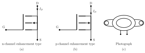
Figure 9.1.12 (titled "MOSFET" in the corrigendum) shows the n-channel and p-channel enhancement-type circuit symbols — drain D, source S and insulated gate G — and a photograph of a real power MOSFET. In the printed book this figure appeared without a caption; the figure number is confirmed by th …
Drawn by us to help you understand the concept clearly, and verified to make sure it's accurate. For exams, practice from your textbook's own diagram.
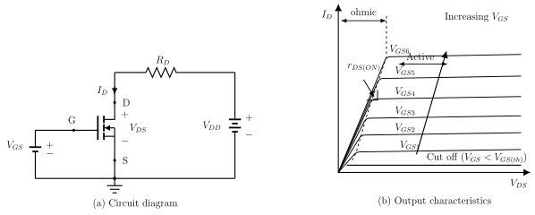
Figure 9.1.13 shows the MOSFET test circuit and the versus output curves for increasing , marking the ohmic region (with ), the active region and cut-off. Following the corrigendum, the source terminal in the circuit is shown grounded …
Drawn by us to help you understand the concept clearly, and verified to make sure it's accurate. For exams, practice from your textbook's own diagram.
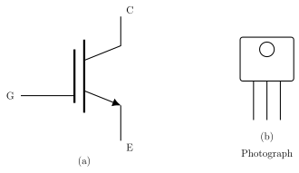
Figure 9.1.14 shows the IGBT circuit symbol — a MOSFET-style insulated gate with a BJT-style emitter arrow, terminals collector C, gate G and emitter E — and a photograph of a real IGBT package. It combines the high input impedance of a MOSFET (voltage-controlled, insulated …
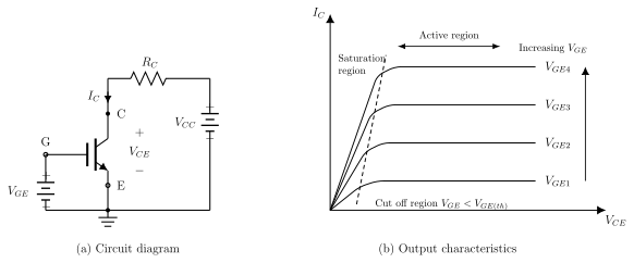
Drawn by us to help you understand the concept clearly, and verified to make sure it's accurate. For exams, practice from your textbook's own diagram.
Figure 9.1.15 shows the IGBT test circuit and the versus output curves for increasing , marking the cut-off, active and saturation regions. Following the corrigendum, the emitter is shown grounded (the p …
The forward drop equals the p+ n- junction drop plus the ohmic drop across the drift region, where is the on-resistance and the forward current. The linear ohmic term is what …
Here is the reverse saturation current, the applied voltage, , a …
With the gate open : With a gate current applied : As the anode …
The lightly doped n- region (about ) placed between the heavily doped p+ anode and n+ cathode of a power diode. Its low charge density gives the wide depletion region need …
The large rise in conductivity of the lightly doped drift region under high forward bias, caused by double injection — holes from the p+ region and electrons from the n+ region flooding the drift layer — which …
The minimum anode current required to keep a thyristor in its on-state immediately after it has been turned on and the gate signal has been removed. It is larger than the holding current, so the anode current must climb above before a short trigger pulse is removed, otherwise the …
The minimum anode current required to keep a thyristor conducting while gate current is applied. The holding current is smaller than the latching current. If the anode current falls below , the thyristor turns off and returns to its forward-blocking state — which is how an SCR is switch …
In a non-punch-through diode the reverse depletion layer stops before the n+ cathode and the electric field falls to zero within the drift region. In a punch-through diode the depletion layer spans the whole drift region and reaches the n+ cathode, so th …