Q.An a.c. source 20sinωt (volts) is connected through a series resistor to a pair of output terminals. Across the output is a branch of an ideal diode in series with a 5V battery: the diode's anode faces the upper output line and its cathode connects to the positive terminal of the 5V battery, whose negative terminal returns to the lower output line — so the diode's cathode is held at +5V with respect to the return line. The output is taken across this diode-battery branch. Assuming the diode is ideal, describe the output waveform and explain it.
🔒You're viewing a preview — the full solution, concept, methods & PYQ mapping are locked.
🔒 Start your 14-day free trial to unlock the full solution →Concept understanding — P-N Junction Rectification
P-N Junction Rectification: Turning AC into DC
Imagine you have a water pipe with a one-way valve. Water can flow freely in one direction, but if you try to push it the other way, the valve slams shut and nothing moves. That's exactly what a p-n junction does — but with electric current instead of water.
The Intuition: Why Does It Let Current Flow Only One Way?
A p-n junction is made by joining two pieces of semiconductor: one p-type (with extra "holes" — think of them as positive charge carriers) and one n-type (with extra electrons). At the junction, something interesting happens.
Electrons from the n-side diffuse into the p-side, and holes from the p-side diffuse into the n-side. They meet and recombine, leaving behind a region with no free charge carriers — the depletion region. This region acts like a tiny battery, creating an internal electric field that points from n to p.
Now here's the key: this internal field opposes the flow of majority carriers. It's like a spring that's been compressed — it wants to push things back.
The depletion region is the reason a p-n junction conducts in only one direction. It's the "gatekeeper."
Forward Bias: Opening the Gate
Connect the p-side to the positive terminal of a battery and the n-side to the negative terminal. This is forward bias.
The external battery pushes holes from p toward n, and electrons from n toward p. They both march toward the depletion region. If the battery voltage is large enough (about 0.7 V for silicon), it overcomes the internal field. The depletion region shrinks, and current flows easily.
Think of forward bias as pushing the spring in the direction it wants to go — it compresses easily, and current flows.
Reverse Bias: Locking the Gate
Now swap the battery: p-side to negative, n-side to positive. This is reverse bias.
The battery pulls holes away from the junction on the p-side, and electrons away on the n-side. The depletion region widens — the spring stretches. No current flows (except a tiny leakage current from minority carriers, which we ignore for now).
If you apply too much reverse voltage, the junction breaks down and current surges. This is avalanche breakdown — it can destroy the diode unless it's designed for it (like a Zener diode).
The Precise Statement
Rectification: A p-n junction diode allows current to flow freely under forward bias and blocks current under reverse bias. This property converts alternating current (AC) into pulsating direct current (DC).
Mathematically, the current-voltage relationship is given by the Shockley diode equation:
I=IS(enVTV−1)
Where:
- I = diode current
- IS = reverse saturation current (tiny, typically 10−12 to 10−6 A)
- V = applied voltage (positive for forward bias, negative for reverse)
- n = ideality factor (usually 1 for ideal, 1–2 for real diodes)
- VT = thermal voltage ≈25.85 mV at room temperature (300 K)
For forward bias (V>0), the exponential term dominates, so I≈ISeV/(nVT) — current grows rapidly.
For reverse bias (V<0), eV/(nVT)≈0, so I≈−IS — a tiny constant leakage current.
How Rectification Works in Practice …
The diode conducts only when the output tries to exceed +5V, clamping it there; otherwise the output equals 20sinωt. So the positive crest is clipped flat at +5V and the negative half is untouched. …
The diode conducts only when the output line tries to rise above +5V (set by the battery), clamping it there; at all other times the diode is off and the output simply follows 20sinωt. The result is the input sine wave with its positive crest flattened at +5V, while the negative half-cycle passes unchanged to −20V — a positive clipper.
Concept
The ideal diode's cathode is held at +5V by the battery. The diode conducts only when its anode (the output line) exceeds its cathode, i.e. when the output would go above +5V; then it clamps the output at +5V. When it is off, no current flows in the series resistor, so there is no IR drop and the output equals the source 20sinωt.
Tracing one cycle
Let v=20sinωt.
- From v=0 rising: the output follows v until v=5V, which occurs at sinωt=0.25 (about ωt=14.5∘).
- For v>5V (through the crest at +20V and back): the diode conducts and the output is held flat at +5V. …
Method: Tracing a Battery-Clamped Diode Clipper Through One Cycle
Step 1 -- Identify the diode's conduction condition.
The diode's cathode is held at a fixed +5 V by the battery. An ideal diode conducts only when its anode (here, the output/source line) rises above its cathode -- i.e. only when the source voltage tries to exceed +5 V.
Step 2 -- Determine the output while the diode is OFF.
When the source is below +5 V, the diode is reverse-biased and carries no current. With no current, there is no drop across the series resistor, so the output simply equals the source: vout=20sinωt.
Step 3 -- Determine the output while the diode is ON.
Once the source tries to exceed +5 V, the diode conducts and clamps the output line to exactly +5 V (ideal diode, zero forward drop); any excess source voltage above 5 V is dropped across the series resistor instead of appearing at the output.
Step 4 -- Trace one full cycle of v=20sinωt. …
- COMEDK 2025Set 2025-E1 markMCQQ.What is the dc component of the output voltage if a sinusoidal signal of 33 V peak voltage is the input of a half wave diode rectifier circuit? (A) 3.5 V (B) 2.9 V (C) 10.5 V (D) 12.5 V
›Reveal solutionSolution
For a half‑wave rectifier with a sinusoidal input of peak voltage Vm, the DC (average) component is Vdc=Vm/π. With Vm=33V, the result is 33/π≈10.5V, so the correct option is (C).
The key concept is average value of a rectified waveform. A half‑wave rectifier passes only the positive half of the input sine wave, blocking the negative half. The DC component is simply the average (mean) of this chopped waveform over one full cycle. For a sine wave, the average of the positive half alone is not half the peak — it’s the peak divided by π. This comes from integrating the sine function over half a period and dividing by the full period.
- Set up the input signal The input is a sinusoidal voltage:
vin(t)=Vmsin(ωt),Vm=33V
where ω=2πf is the angular frequency.
- Define the half‑wave rectified output For an ideal diode, the output voltage vo(t) equals the input during the positive half‑cycle (when sin(ωt)≥0) and is zero during the negative half‑cycle. So over one period T=2π/ω:
vo(t)={Vmsin(ωt),0,0≤ωt≤ππ≤ωt≤2π
- Compute the DC (average) value The average of a periodic waveform over one period is:
Vdc=T1∫0Tvo(t)dt
Substituting the half‑wave expression:
Vdc=T1∫0T/2Vmsin(ωt)dt
Let θ=ωt, so dt=dθ/ω and the limits become 0 to π. Then:
Vdc=2π1∫0πVmsinθdθ
The integral of sinθ from 0 to π is 2. Hence:
- COMEDK 2024Set 2024-E1 markMCQQ.The output of the given circuit is A. Negatively rectified half wave B. Positively rectified half wave C. Negatively rectified full wave D. Zero all times (A) B (B) D (C) A (D) C
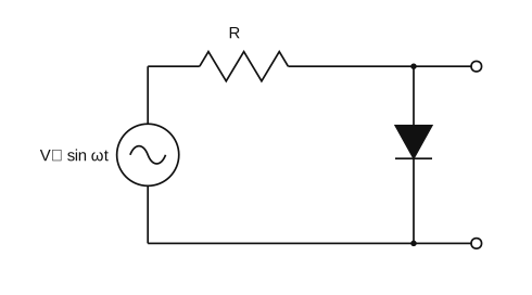
›Reveal solutionSolution
The shunt diode shorts the positive half-cycles and passes the negative ones, giving a negatively rectified half-wave output — statement A, i.e. answer choice (C).
Circuit: AC source, resistor R in series in the top wire, and a diode connected across the two open output terminals (in shunt). The triangle's base is up and its apex points down, so the anode is at the top node and the cathode at the bottom rail — the diode conducts when the top node is positive.
- Positive half-cycle (top node positive): diode is forward biased, effectively a short across the output, so Vout≈0. …
- COMEDK 2024Set 2024-M1 markMCQQ.An ideal diode is connected in series with a capacitor. The free ends of the capacitor and the diode are connected across a 220 V ac source. Now the potential difference across the capacitor is : (A) 110 V (B) 311 V (C) 2110 V (D) 220 V
›Reveal solutionSolution
The diode rectifies the AC, charging the capacitor to the peak voltage of the source, which is 2202≈311 V. The correct option is (B).
Concept & Intuition
An ideal diode allows current to flow only in one direction. When connected in series with a capacitor across an AC source, the diode acts as a half-wave rectifier. During the half-cycle when the diode is forward-biased, the capacitor charges up to the peak voltage of the AC source. Once charged, the diode becomes reverse-biased on the next half-cycle and blocks discharge, so the capacitor holds that peak voltage. The key is to distinguish between the RMS voltage (given as 220 V) and the peak voltage, which is what actually appears across the capacitor.
Step-by-step reasoning
- Identify the source voltage form The AC source is 220 V RMS. For a sinusoidal voltage, the peak voltage Vpeak is related to the RMS value by
Vpeak=VRMS×2.
So here,
Vpeak=220×2≈311 V.
-
Understand the diode’s action
During the positive half-cycle (when the anode is positive relative to the cathode), the diode is forward-biased and conducts. Current flows through the diode and charges the capacitor to the instantaneous voltage of the source.
During the negative half-cycle, the diode is reverse-biased and acts as an open circuit — no current flows. The capacitor cannot discharge through the diode, and if we assume no other load, it retains its charge.
-
What voltage does the capacitor reach?
The capacitor charges only during the first positive half-cycle. It will charge up to the maximum voltage the source reaches during that half-cycle, which is the peak voltage Vpeak. After that, the diode blocks any reverse current, so the capacitor holds this peak voltage indefinitely (assuming ideal components with no leakage).
-
Check the options …
- COMEDK 2021Set 2021-B1 markMCQQ.Assume the diode D is ideal, the output voltage waveform across R1 is V0, then V0 is [FIGURE: a half-wave rectifier circuit — an AC source e=10sin100πt in parallel with load resistor R1 through an ideal diode D, and the output waveform showing rectified half-sine pulses] (A) 10 V (B) 14.1 V (C) 10/2 V (D) 5 V
›Reveal solutionSolution
The half-wave rectified output peaks at the source peak, 10 V.
The source is e=10sin100πt, so its peak voltage is Vm=10V. With an ideal diode (no forward drop), during the conducting half-cycle the full source voltage appears across R1, and during the blocking half-cycle the output is zero. …
- KCET 2018Set A-11 markMCQQ.In a CE amplifier, the input ac signal to be amplified is applied across (A) Forward biased emitter-base junction (B) Reverse biased collector-base junction (C) Reverse biased emitter-base junction (D) Forward biased collector-base junction
›Reveal solutionSolution
A transistor amplifier is always biased with the emitter–base junction FORWARD and the collector–base junction REVERSE; the ac signal to be amplified rides on the forward-biased input (emitter–base) junction.
Step 1 — The active-region biasing rule.
For a transistor to work as an amplifier it must be in the active region, which requires:
- emitter–base junction: FORWARD biased (so the heavily doped emitter injects a large carrier current into the thin, lightly doped base);
- collector–base junction: REVERSE biased (so the collector sweeps up almost all of those injected carriers).
Step 2 — Where the signal goes in CE configuration.
In the common-emitter configuration the emitter is common to input and output. The input is between base and emitter, so the ac signal to be amplified is applied across the forward-biased emitter–base junction (superposed on its dc bias VBE). The output is taken between collector and emitter, across the reverse-biased collector–base side.
Step 3 — Why this produces amplification.
The input junction is forward biased, so its dynamic resistance is small; the output junction is reverse biased, so its resistance is large. A tiny signal voltage on the low-resistance input produces a base-current swing ΔIB, which produces a much larger collector-current swing ΔIC=βΔIB through the large output-side load resistance RL. Hence …
🎓Unlock everything free for 14 days
- ✓Full step-by-step solutions
- ✓Concept-first explanations
- ✓Methods, shortcuts & mistakes
- ✓PYQ mapping + timed mock tests
Full access for 14 days. No credit card required.