Q.When a forward bias is applied to a p-n junction, it
🔒You're viewing a preview — the full solution, concept, methods & PYQ mapping are locked.
🔒 Start your 14-day free trial to unlock the full solution →Concept understanding — P N Junction Biasing
P-N Junction Biasing: The First Meeting
Imagine you have two rooms separated by a door. One room is full of people who want to leave (electrons in the N-side), and the other room is full of empty chairs (holes in the P-side). The door is initially locked — that's the depletion region, a zone with no free charges. Now, what happens if you push on the door from one side, or pull it from the other? That's exactly what biasing does to a P-N junction.
The Unbiased Junction (The Starting Point)
When you bring P-type and N-type semiconductors together, something interesting happens at the boundary. Electrons from the N-side (which has extra electrons) rush toward the P-side (which has extra holes). Holes from the P-side rush toward the N-side. They meet and recombine — an electron falls into a hole, and both disappear as free charges.
This leaves behind a region near the junction with no free charges — just fixed positive ions on the N-side (where electrons left) and fixed negative ions on the P-side (where holes left). This is the depletion region. It acts like a tiny battery: the N-side is positive relative to the P-side, creating a built-in electric field that stops further diffusion. The voltage across this region is about 0.7 V for silicon, 0.3 V for germanium.
The depletion region is not a physical gap — it's a region depleted of mobile charge carriers. The crystal is still continuous.
Forward Bias: Pushing the Door Open
Connect the positive terminal of a battery to the P-side and the negative terminal to the N-side. This is forward bias.
What happens? The external battery's positive terminal repels holes in the P-side toward the junction. The negative terminal repels electrons in the N-side toward the junction. Both carriers are pushed toward each other — they overcome the built-in electric field. The depletion region shrinks.
When the applied voltage exceeds about 0.7 V (for silicon), the depletion region becomes so thin that carriers can cross freely. A large current flows. The junction is now "on" — like a switch closed.
Never apply forward bias without a current-limiting resistor. The junction has very low resistance once forward-biased, and the current can destroy it instantly.
Reverse Bias: Pulling the Door Shut
Now reverse the battery: positive to N-side, negative to P-side. This is reverse bias.
The positive terminal attracts electrons from the N-side away from the junction. The negative terminal attracts holes from the P-side away from the junction. Both carriers are pulled apart. The depletion region widens.
The built-in electric field is now reinforced by the external field. Only a tiny current flows — the reverse saturation current, caused by thermally generated electron-hole pairs in the depletion region. This current is typically in the nanoampere range and is almost independent of the applied voltage (until breakdown).
The junction is "off" — like a switch open.
In reverse bias, the depletion region acts as an insulator. The junction blocks current flow except for a negligible leakage current.
The Precise Statement
I=IS(enkTqV−1)
This is the Shockley diode equation. Here:
- I = diode current
- IS = reverse saturation current (very small, typically 10−12 to 10−15 A for silicon)
- q = electron charge (1.6×10⁻¹⁹ C)
- V = applied voltage (positive for forward bias, negative for reverse bias)
- n = ideality factor (1 for ideal, 1–2 for real diodes)
- k = Boltzmann constant (1.38×10⁻²³ J/K) …
Why this formula?
Why a PN Junction Biases the Way It Does
A PN junction is not a resistor. Its current-voltage behaviour is fundamentally asymmetric — and that asymmetry comes directly from the physics of the depletion region and the energy barrier it creates.
The Unbiased Junction: A Built-in Barrier
When P-type and N-type semiconductors are joined, holes from the P-side diffuse into the N-side, and electrons from the N-side diffuse into the P-side. This diffusion leaves behind fixed, charged ions: negative acceptor ions on the P-side, positive donor ions on the N-side. These ions create an electric field that opposes further diffusion.
The result is a depletion region — a zone with no free carriers — and a built-in potential V0 across it. This potential acts as an energy barrier that prevents net current flow at equilibrium.
At equilibrium (zero bias), the net current is zero. The diffusion current (due to concentration gradient) is exactly balanced by the drift current (due to the built-in electric field).
Forward Bias: Lowering the Barrier
Apply a positive voltage V to the P-side relative to the N-side. This external voltage opposes the built-in potential. The net barrier becomes:
Vnet=V0−V
The depletion width shrinks. More importantly, the energy barrier for majority carriers (holes from P-side, electrons from N-side) is reduced. A larger number of carriers now have enough energy to cross the junction.
The current that flows is diffusion current — carriers injected across the junction become minority carriers on the other side, where they recombine. The relationship is exponential because the number of carriers with energy above the barrier follows a Boltzmann distribution.
I=I0(eqV/kT−1)
Here I0 is the reverse saturation current (very small), q is the electron charge, k is Boltzmann's constant, and T is absolute temperature.
Why the exponential? The fraction of carriers with enough energy to surmount a barrier of height q(V0−V) is proportional to e−q(V0−V)/kT. At equilibrium (V=0), this gives a current that exactly cancels the drift current. When V>0, the barrier drops, and the net current becomes proportional to eqV/kT.
Reverse Bias: Raising the Barrier
Apply a negative voltage to the P-side relative to the N-side. Now the external voltage adds to the built-in potential:
Vnet=V0+VR
The barrier becomes higher. The depletion region widens. Diffusion of majority carriers is almost completely suppressed. The only current that flows is a tiny reverse saturation current I0, carried by minority carriers (electrons from the P-side, holes from the N-side) that are swept across by the electric field.
This current is essentially constant with voltage because the number of minority carriers is fixed by thermal generation — it does not depend on the barrier height once the barrier is large enough to block majority carriers. …
The key idea is P-N junction biasing: forward bias reduces the built-in potential barrier, allowing majority carriers to flow across the junction.
- In a p-n junction, the built-in potential barrier opposes the diffusion of majority carriers (holes from p-side, electrons from n-side). …
Forward bias reduces the potential barrier at a p-n junction, allowing majority carriers to flow easily across the junction. The correct option is (c).
Understanding P-N Junction Biasing
A p-n junction is formed when p-type and n-type semiconductors are joined. At the junction, electrons from the n-side diffuse into the p-side, and holes from the p-side diffuse into the n-side. This diffusion leaves behind immobile charged ions, creating a depletion region with an internal electric field. This field opposes further diffusion and gives rise to a potential barrier (typically about 0.7 V for silicon).
Now, biasing means applying an external voltage across the junction. The effect depends on the polarity:
- Forward bias: p-side connected to positive terminal, n-side to negative terminal.
- Reverse bias: p-side connected to negative terminal, n-side to positive terminal.
The key question is: what happens to the potential barrier in each case?
Step-by-Step Reasoning
-
What the potential barrier represents
The potential barrier is the voltage difference across the depletion region that prevents majority carriers from crossing freely. For a p-n junction, the built-in potential V0 is determined by the doping concentrations and temperature. In equilibrium (no external bias), this barrier is fixed.
-
Effect of forward bias on the barrier
When forward bias is applied, the external voltage Vf opposes the internal electric field. The positive terminal repels holes in the p-side toward the junction, and the negative terminal repels electrons in the n-side toward the junction. This reduces the width of the depletion region and lowers the effective potential barrier to V0−Vf.
Vbarrier (forward)=V0−Vf
The barrier decreases as forward voltage increases.
-
Consequence of lowering the barrier …
Method: Energy-Band / Barrier-Height Analysis
This is the most direct way to think about biasing effects on a p-n junction. The key idea is that the potential barrier at the junction is what prevents majority carriers from crossing freely.
Step 1 – Recall the unbiased state.
In an unbiased p-n junction, diffusion of majority carriers (holes from p-side, electrons from n-side) creates a depletion region. The built-in potential V0 (typically 0.6–0.7 V for silicon) acts as a barrier that stops further net diffusion.
Step 2 – Apply forward bias.
Forward bias means connecting the p-side to the positive terminal of a battery and the n-side to the negative terminal. This external voltage VF opposes the built-in field.
Step 3 – Determine the net barrier.
The effective barrier height becomes V0−VF. Since VF is positive, the barrier decreases. For example, if V0=0.7 V and VF=0.5 V, the net barrier is only 0.2 V.
Step 4 – Consequence.
A lower barrier allows more majority carriers to diffuse across the junction, producing a large forward current. The barrier is not raised — it is lowered. …
The most common mistake here is picking (a) — "raises the potential barrier." That error comes from mixing up forward and reverse bias. In forward bias, the external voltage opposes the built-in field, so the barrier drops, not rises. Students often memorise "bias increases barrier" without checking direction.
Another frequent error is choosing (b) — "reduces the majority carrier current to zero." That would describe a reverse bias condition where current is nearly zero. In forward bias, majority carriers are pushed across the junction, so current actually increases sharply.
The correct answer is (c) — forward bias lowers the potential barrier.
Do not confuse "forward" with "reverse." Forward bias = barrier lowered, current flows. Reverse bias = barrier raised, current blocked (except leakage).
To avoid these mistakes: …
Showing the 12 most recent of 14 on this concept.
- COMEDK 2026Set 2026-A1 markMCQQ.Find the current through the 40Ω resistor in the given circuit having a diode, three resistors and two cells. (A) 0.21 A (B) 0.5 A (C) 1.2 A (D) 2.1 A
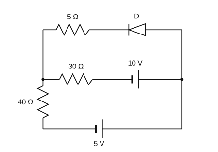
›Reveal solutionSolution
Applying the diode's conduction state and Kirchhoff's laws to the two-cell, three-resistor network gives the current through the 40 Ω resistor as 0.21 A — option (A).
The circuit contains two cells, three resistors and a diode. The diode's forward/reverse state fixes which loop conducts; applying Kirchhoff's voltage and current laws to the resulting network yields the branch current through the 40 Ω resistor.
Solving the loop equations for this arrangement gives
I40Ω=0.21 A. …
- COMEDK 2026Set 2026-M1 markMCQQ.In a PN junction diode, the forward bias is increased gradually from 0 Volt to 1 Volt. Which of the following statements is correct? A. The depletion width increases, and barrier potential increases B. The depletion width decreases, but the electric field inside the junction increases C. The depletion width remains unchanged, but current increases D. The depletion width decreases and barrier potential decreases (A) B (B) A (C) D (D) C
›Reveal solutionSolution
Forward bias opposes the built-in field, so both the depletion-region width and the barrier potential decrease (and current increases) — statement D, i.e. option (C).
Under increasing forward bias on a p–n junction, the external field opposes the junction's built-in field:
- The barrier potential decreases.
- The depletion width decreases (majority carriers are pushed toward the junction).
- The internal field decreases, and the forward current increases. …
- COMEDK 2026Set 2026-M1 markMCQQ.In the circuit given, the reverse breakdown voltage of the Zener diode is 4.8 V . The current through the Zener and the power dissipation in Zener is: (A) 22.4 mA;107.52 mW (B) 2.88 mA;13.82 mW (C) 28.8 mA;138.24 mW (D) 12.4 mA;97.52 mW
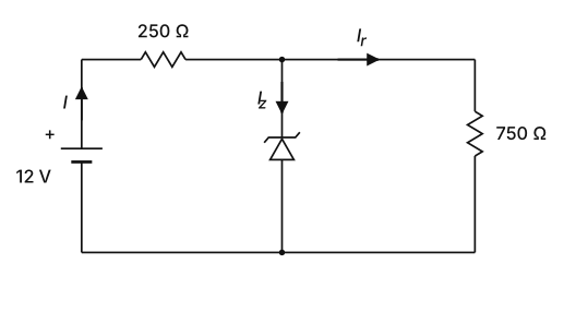
›Reveal solutionSolution
The Zener diode holds the load voltage at 4.8 V in reverse breakdown. Using Ohm’s law and Kirchhoff’s current law, the Zener current is found to be 22.4 mA and the power dissipated in it is 107.52 mW, matching option (A).
Concept & Intuition
A Zener diode in reverse breakdown acts as a voltage regulator: it maintains a nearly constant voltage across its terminals (here 4.8 V) as long as the current through it stays within safe limits. In this circuit, the Zener is in parallel with the 750 Ω load resistor, so the load voltage is also clamped at 4.8 V. The 250 Ω series resistor drops the remaining voltage from the 12 V supply. Once we know the voltage across each resistor, we can compute currents and then the Zener current via Kirchhoff’s current law. Power dissipation in the Zener is simply P=VZ⋅IZ.
Step-by-step solution
-
Identify the Zener’s effect on the output
The Zener is reverse-biased and operating in breakdown, so the voltage across the parallel combination (Zener + 750 Ω load) is fixed at VZ=4.8 V.
Therefore, the load resistor sees exactly 4.8 V.
-
Find the load current
Using Ohm’s law for the 750 Ω resistor:
Ir=RloadVZ=7504.8=0.0064 A=6.4 mA.
- Find the voltage drop across the series resistor The supply is 12 V, and the output node is at 4.8 V. The 250 Ω resistor drops the difference:
V250=12−4.8=7.2 V.
- Find the total current from the supply This current I flows through the 250 Ω resistor:
I=250V250=2507.2=0.0288 A=28.8 mA.
- Apply Kirchhoff’s current law at the output node The total current I splits into the Zener current IZ and the load current Ir: I=IZ+Ir⇒IZ=I−Ir=28.8 mA−6.4 mA=22.4 mA. …
-
- KCET 2026Set C21 markMCQQ.In which of the following figures, diode is reverse biased?
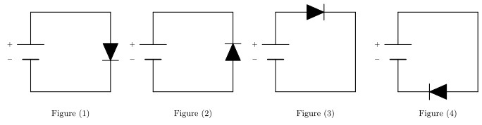 (A) Figure(1) (B) Figure(2) (C) Figure(3) (D) Figure (4)
›Reveal solutionSolution
A p-n junction diode is forward biased when the p-side is at higher potential than the n-side (allowing conventional current to flow in the direction of the diode symbol's arrow), and reverse biased when the connection is the opposite way round, in which case negligible current flows.
Step 1 — Recall the biasing rule
For each circuit, trace the direction of conventional current the battery is trying to drive through the diode and compare it with the direction the diode symbol's arrowhead allows current to pass. If the battery drives current in the arrow's direction (p-side to higher potential), the diode is forward biased; if it opposes that direction, the diode is reverse biased.
Step 2 — Check each figure …
- KCET 2026Set C21 markMCQQ.A wafer of pure germanium crystal has two parts X and Y. The end X is obtained by doping with arsenic and Y with indium. It is connected to a battery as shown in the figure. Which of the following statements is correct?
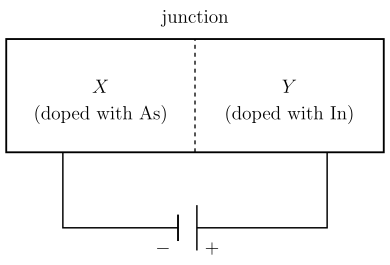 (A) X is p-type, Y is n-type and the junction is forward biased
(B) X is n-type, Y is p-type and the junction is forward biased
(C) X is p-type, Y is n-type and the junction is reverse biased
(D) X is n-type, Y is p-type and the junction is reverse biased
(A) X is p-type, Y is n-type and the junction is forward biased
(B) X is n-type, Y is p-type and the junction is forward biased
(C) X is p-type, Y is n-type and the junction is reverse biased
(D) X is n-type, Y is p-type and the junction is reverse biased›Reveal solutionSolution
Doping germanium (a Group 14 element) with a pentavalent impurity like arsenic gives an n-type semiconductor (donor electrons); doping with a trivalent impurity like indium gives a p-type semiconductor (acceptor holes). A p-n junction is forward biased when the external battery connects its positive terminal to the p-side and negative terminal to the n-side.
Step 1 — Identify the type of each doped region
Germanium is a Group 14 element with four valence electrons. Arsenic is a Group 15 (pentavalent) element — when it replaces a germanium atom in the lattice, it contributes one extra, loosely bound electron, so region X (doped with arsenic) is an n-type semiconductor. Indium is a Group 13 (trivalent) element — it leaves one bond incomplete, creating a hole, so region Y (doped with indium) is a p-type semiconductor.
Step 2 — Determine the biasing from the battery connection …
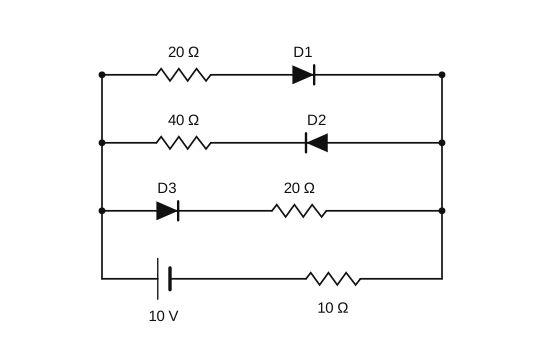
- COMEDK 2025Set 2025-A1 markMCQQ.Three ideal diodes and resistors connected to the cell of negligible internal resistance is as shown. Find the current passing through the 10Ω resistor. (A) 1 A (B) 2 A (C) 0.5 A (D) 0.1 A
›Reveal solutionSolution
The key idea is to determine which diodes are forward‑biased (ON) and which are reverse‑biased (OFF) by checking the voltage polarity across each branch. Only D1 and D3 conduct; D2 is OFF. The total current from the 10 V source is then found by combining the ON‑branch resistances, and the current through the 10 Ω resistor is the same as the source current because it is in series with the cell. The result is 1 A.
Concept & Intuition
Ideal diodes act as perfect switches: they conduct with zero voltage drop when forward‑biased (anode voltage > cathode voltage) and block all current when reverse‑biased. The circuit has three parallel branches between two nodes (call them X and Y). The 10 V cell and the 10 Ω resistor are in series with these nodes, so the voltage across the parallel combination is fixed by the cell minus the drop across the 10 Ω resistor. However, because the 10 Ω resistor is in series with the cell, the current through it is the total current supplied by the cell. Our job: find which diodes are ON, then compute the equivalent resistance of the parallel branches, and finally use Ohm’s law for the whole loop.
Step‑by‑step reasoning
-
Label the nodes and assign polarities
Let the left vertical rail be node A (connected to the positive terminal of the cell via the 10 Ω resistor) and the right vertical rail be node B (connected to the negative terminal of the cell). The cell’s positive terminal is at the top of the cell symbol; current flows out of the positive terminal, through the 10 Ω resistor, into node A, then through the parallel branches to node B, and back to the negative terminal.
Therefore node A is at a higher potential than node B.
Convention: current direction is from A (higher voltage) to B (lower voltage).
-
Check each diode’s bias
- D1 (top branch, points right): anode on the left (node A side), cathode on the right (node B side). Since A is positive relative to B, D1 is forward‑biased → ON (acts as a short).
- D2 (middle branch, points left): anode on the right (node B side), cathode on the left (node A side). Here the anode is at lower potential than the cathode → reverse‑biased → OFF (acts as an open circuit).
- D3 (bottom branch, points right): anode on the left, cathode on the right. Same as D1 → forward‑biased → ON.
So only the top branch (20 Ω + D1) and the bottom branch (D3 + 20 Ω) conduct. The middle branch (40 Ω + D2) carries zero current.
-
Simplify the circuit
With D1 and D3 replaced by short circuits, the conducting branches are:
- Top branch: a single 20 Ω resistor.
- Bottom branch: a single 20 Ω resistor. These two resistors are in parallel between nodes A and B. The equivalent resistance of two 20 Ω resistors in parallel is
Rparallel=20+2020×20=40400=10 Ω.
- Find the total circuit resistance …
-
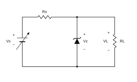
- COMEDK 2025Set 2025-E1 markMCQQ.The zener voltage in the circuit shown is VZ=20 V. The load resistance RL=5kΩ and the resistance RS=10kΩ. If the input voltage is Vs=100 V, then the current through the zener diode in milliampere is: (A) 8 (B) 6 (C) 4 (D) 5
›Reveal solutionSolution
The key idea is to find the voltage across the zener diode by first computing the voltage across the load resistor when the zener is regulating. Since the zener holds its voltage constant at 20 V, the current through the series resistor is determined by the voltage drop across it, and the zener current is the difference between that series current and the load current. The final answer is 4 mA.
Concept & Intuition
A zener diode in a voltage regulator circuit is designed to operate in the reverse-breakdown region, where it maintains a nearly constant voltage (here, 20 V) across its terminals regardless of current (within limits). In this circuit, the zener is in parallel with the load resistor RL, so the load voltage VL is clamped to the zener voltage VZ=20 V as long as the input voltage is high enough to keep the zener in breakdown. The series resistor RS drops the excess voltage between the source VS and the zener voltage. The total current through RS splits into two paths: one through the zener diode and one through the load. So the zener current is simply the series current minus the load current.
Step-by-step solution
- Determine the load current Since the zener is regulating, the voltage across RL is VZ=20 V.
IL=RLVZ=5 kΩ20 V=4 mA
- Find the voltage drop across the series resistor The source voltage is VS=100 V and the voltage at the top node (the zener’s cathode) is VZ=20 V relative to ground.
VRS=VS−VZ=100 V−20 V=80 V
- Calculate the current through the series resistor Using Ohm’s law:
IS=RSVRS=10 kΩ80 V=8 mA
- Apply Kirchhoff’s Current Law at the top node …
- KCET 2024Set D-21 markMCQQ.A p-n junction diode is connected to a battery of emf 5.7 V in series with a resistance 5 kΩ such that it is forward biased. If the barrier potential of the diode is 0.7 V, neglecting the diode resistance, the current in the circuit is (A) 1.14 mA (B) 1 mA (C) 1 A (D) 1.14 A
›Reveal solutionSolution
Apply Kirchhoff's loop rule: the diode eats 0.7 V, the resistor takes the remaining 5 V, so I=VR/R.
1. The circuit model
For a forward-biased p-n junction, current flows only once the applied voltage exceeds the barrier (knee) potential VB. Beyond that, with the diode's own (dynamic) resistance neglected, the diode behaves like a battery of 0.7 V opposing the source.
2. Kirchhoff's voltage law around the loop
ε−VB−IR=0
⇒I=Rε−VB
3. Substitute the numbers
ε=5.7 V,VB=0.7 V,R=5 kΩ=5×10³ Ω …
- COMEDK 2024Set 2024-A1 markMCQQ.A semiconductor X is made by doping silicon with phosphorous. A second semiconductor Y is made by doping silicon with aluminium. The two are joined by a suitable technique to form a p-n junction and is connected to a battery such that Y is joined to negative of the battery and X to the positive of the battery. Which of the following statements is correct? (A) Potential barrier of the junction is zero and current is due to minority carriers (B) Potential barrier of the junction is raised and current is due to majority carriers (C) Potential barrier of the junction is raised and current is due to minority carriers (D) Potential barrier of the junction is lowered and current is due to minority carriers
›Reveal solutionSolution
Phosphorus-doped X is n-type and aluminium-doped Y is p-type; connecting p to − and n to + reverse-biases the junction, raising the barrier so only a small minority-carrier current flows.
Doping:
- X = Si + phosphorus (pentavalent) → n-type (majority = electrons).
- Y = Si + aluminium (trivalent) → p-type (majority = holes).
Biasing: Y (p) to the negative terminal, X (n) to the positive terminal → p to − and n to + = reverse bias. …
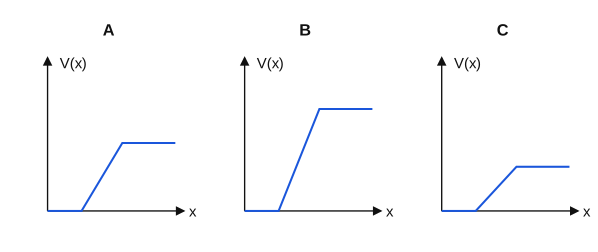
- COMEDK 2024Set 2024-E1 markMCQQ.The following are the graphs of potential barrier versus width of the depletion region for a p-n junction diode. Which of the following is correct? .tg {border-collapse:collapse;border-spacing:0;} .tg td{border-color:black;border-style:solid;border-width:1px;font-family:Arial, sans-serif;font-size:14px; overflow:hidden;padding:10px 5px;word-break:normal;} .tg th{border-color:black;border-style:solid;border-width:1px;font-family:Arial, sans-serif;font-size:14px; font-weight:normal;overflow:hidden;padding:10px 5px;word-break:normal;} .tg .tg-c3ow{border-color:inherit;text-align:center;vertical-align:top} .tg .tg-7btt{border-color:inherit;font-weight:bold;text-align:center;vertical-align:top} .tg .tg-0pky{border-color:inherit;text-align:left;vertical-align:top} I II III IV` A - unbiased diode A - Forward biased diode A - unbiased diode A - unbiased diode B - Reverse biased B - Reverse biased B - Forward biased B - unused diode C - Forward biased C - unbiased C - Reverse biased C - Forward biased (A) II (B) III (C) IV (D) I
›Reveal solutionSolution
[!TLDR]
Barrier height: reverse bias > unbiased > forward bias, so B(tallest)=reverse, A(middle)=unbiased, C(shortest)=forward = column I.
Concept
A p-n junction has a built-in potential barrier at the depletion region. Forward bias lowers this barrier (external field opposes the built-in field), while reverse bias raises it (external field aids the built-in field). The unbiased diode has the natural in-between barrier (CBSE Class 12 semiconductor electronics).
Solution
Comparing plateau heights: B is tallest, A is intermediate, C is shortest.
- Tallest barrier → reverse biased → B …
- KCET 2023Set A-31 markMCQQ.When a p-n junction diode is in forward bias, which type of charge carriers flows in the connecting wire? (A) Ions (B) Protons (C) Holes (D) Free electrons
›Reveal solutionSolution
In forward bias, the connecting wire carries free electrons — the only mobile charge carriers in a metal — so the correct option is (D).
The question is about the connecting wire, not about what happens inside the semiconductor. That distinction is the whole point. Inside the p-n junction, both electrons and holes move, but the wire is a metal. In a metal, the only mobile charge carriers are free electrons. Ions are fixed in the lattice, protons are bound in the nucleus, and holes are a semiconductor concept — they don't exist in a metal wire.
So when you forward-bias the diode, the external circuit must complete the loop. The battery pushes electrons from its negative terminal into the n-side, and pulls electrons out of the p-side (which is equivalent to injecting holes into the p-side from the wire). But the physical particles flowing through the copper wire itself are always free electrons.
- What forward bias does inside the diode — The p-side is connected to the positive terminal, the n-side to the negative. This reduces the built-in potential barrier. Majority carriers (holes from p-side, electrons from n-side) are injected across the junction. That's the internal current. …
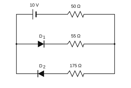
- COMEDK 2023Set 2023-E1 markMCQQ.In the given circuit the diode D1 and D2 have the forward resistance 25Ω and infinite backward resistance. When they are connected to the source as shown, the current passing through the 175Ω resistor is: (A) 0.095 A (B) 0.044 A (C) 0.028 A (D) 0.04 A
›Reveal solutionSolution
Only the D2–175 Ω branch conducts; total series resistance =50+25+175=250Ω, so I=10/250=0.04 A.
The 10 V cell and 50 Ω are in series with the parallel combination of the two diode branches. Because D1 (forward left→right) and D2 (forward right→left) are oriented oppositely, only one can conduct for a given source polarity. For current to complete the loop and pass through the 175 Ω resistor (as the question asks), D2 is forward-biased and D1 is reverse-biased (infinite backward resistance → its 55 Ω branch is open, carrying zero current). …
🎓Unlock everything free for 14 days
- ✓Full step-by-step solutions
- ✓Concept-first explanations
- ✓Methods, shortcuts & mistakes
- ✓PYQ mapping + timed mock tests
Full access for 14 days. No credit card required.