Q.Carbon, silicon and germanium have four valence electrons each. These are characterised by valence and conduction bands separated by energy band gap respectively equal to (Eg)C, (Eg)Si and (Eg)Ge. Which of the following statements is true?
Concept understanding — Band Gap Energy
What is Band Gap Energy? — A First Look
Imagine you have a single atom. Its electrons live in specific, fixed energy levels — like rungs on a ladder. You can't put an electron halfway between two rungs; it's either on one rung or another.
Now bring two atoms close together. Their electron rungs interact and split into two slightly different energies. Bring a billion atoms together — as in a solid crystal — and those original rungs spread into continuous bands of allowed energies, separated by gaps where no electron can exist.
That gap — the forbidden region between two bands — is the band gap.
The Intuition: A Wall Between Two Rooms
Think of the valence band as the ground floor of a building — electrons here are tightly bound to atoms, not free to move. The conduction band is the first floor above — electrons here can roam freely through the crystal, carrying current.
The band gap is the height of the ceiling between these two floors. An electron needs exactly that much energy to jump from the valence band to the conduction band. If you give it less energy, it stays stuck on the ground floor. If you give it exactly the gap energy or more, it can leap up and become a mobile charge carrier.
In a metal, the valence and conduction bands overlap — there is no gap. That's why metals conduct electricity so easily: electrons already have free states available at no energy cost.
The Precise Statement
Band gap energy (Eg) is the minimum energy required to excite an electron from the top of the valence band to the bottom of the conduction band in a solid.
Eg=Econduction band minimum−Evalence band maximum
It is measured in electron volts (eV). One eV is the energy gained by an electron when accelerated through a potential difference of 1 volt — a tiny but convenient unit for atomic-scale energies.
Why Does It Matter?
The band gap determines almost everything about how a material behaves electrically and optically:
| Material type | Typical Eg | Behaviour |
|---|---|---|
| Conductor (metal) | Eg=0 (bands overlap) | Electrons flow freely at room temperature |
| Semiconductor | 0.1 eV<Eg<3 eV | Conducts only when given energy (heat, light) |
| Insulator | Eg>3 eV | Almost no conduction at normal conditions |
A quick rule of thumb: if a material is transparent to visible light, its band gap is larger than about 3.1 eV (the energy of violet light). Diamond (Eg≈5.5 eV) is transparent; silicon (Eg≈1.1 eV) is opaque and shiny.
A Concrete Example: Silicon
Silicon has a band gap of 1.12 eV at room temperature. This means:
- An electron in the valence band needs at least 1.12 eV to jump to the conduction band.
- Visible light photons have energies between 1.8 eV (red) and 3.1 eV (violet). So silicon absorbs most visible light — that's why solar cells are dark.
- At absolute zero, silicon is a perfect insulator. At room temperature, thermal energy (~0.025 eV) is far less than 1.12 eV, but a tiny fraction of electrons still get enough energy from random vibrations to jump the gap — giving silicon its useful semiconducting properties.
Do not confuse band gap energy with the work function. The work function is the energy needed to remove an electron entirely from the solid (into vacuum). Band gap is the energy needed to move an electron from one band to another inside the solid.
The Key Takeaway
Band gap energy is the energy threshold that separates insulating behaviour from conducting behaviour in a solid. It explains why diamond is transparent and silicon is not, why copper conducts electricity effortlessly, and why LEDs emit light of a specific colour (the colour corresponds directly to the band gap energy of the semiconductor).
Band gap energy is a key concept from the NCERT Class 12 Physics Semiconductor Electronics chapter that distinguishes conductors, semiconductors, and insulators, and "band gap energy definition and formula" is a frequently searched topic for CBSE board and JEE Main preparation. This concept also connects directly to LED colour and solar-cell design questions that regularly appear in "semiconductor devices important questions" lists.
Why this formula?
Band Gap Energy: Why the Formula Holds
The band gap energy Eg is the energy difference between the top of the valence band and the bottom of the conduction band in a solid. The key formula is:
Eg=Ec−Ev
where Ec is the minimum energy of the conduction band and Ev is the maximum energy of the valence band.
But why does this simple difference matter? The answer lies in how electrons behave in a crystal.
The Origin of Energy Bands
In an isolated atom, electrons occupy discrete energy levels. When atoms come together to form a solid, their atomic orbitals overlap. According to the Pauli exclusion principle, no two electrons can occupy the same quantum state. So the discrete levels split into a continuum of closely spaced levels — an energy band.
The valence band is formed from the outermost (valence) atomic orbitals. The conduction band is formed from the next higher set of orbitals (typically the empty orbitals above the valence orbitals). Between these bands lies the band gap — a region of forbidden energies where no electron states exist.
Why the Formula Eg=Ec−Ev Is Not Trivial
You might think: "Of course the gap is the difference between the bottom of one band and the top of another." But the real insight is that Ec and Ev are not arbitrary points — they are the extrema of the band structure.
In a periodic crystal, the electron energy E(k) depends on the wavevector k. The valence band has its maximum at some k-point (often at k=0 for direct-gap semiconductors), and the conduction band has its minimum at some k-point. The band gap is:
Eg=minkcEc(kc)−maxkvEv(kv)
This is not just a difference — it's a minimisation over all possible electron momenta.
Why This Difference Determines Conductivity
The band gap controls whether a material is an insulator, semiconductor, or conductor because of the Fermi-Dirac distribution:
f(E)=1+e(E−EF)/kBT1
At absolute zero, all states below the Fermi level EF are filled, and all above are empty. For an intrinsic semiconductor, EF lies in the middle of the band gap. The probability that an electron is thermally excited from the valence band to the conduction band is proportional to e−Eg/2kBT.
The band gap energy Eg appears in the exponent of the carrier concentration formula:
n=p=NcNve−Eg/2kBT
This is why a small change in Eg causes a huge change in conductivity — it's an exponential dependence.
The Physical Meaning of Eg
The band gap is not just a number — it's the minimum energy required to:
- Break a covalent bond in the crystal (creating an electron-hole pair)
- Promote an electron from a bonding state to an antibonding state
- Create a mobile charge carrier
For example, in silicon (Eg=1.12 eV at 300 K), a photon with energy greater than 1.12 eV can be absorbed, exciting an electron from the valence band to the conduction band. This is why silicon is used in solar cells — the band gap matches the solar spectrum.
A common mistake is to think the band gap is simply the difference between the highest and lowest energy levels in the solid. It is not — it is the gap between the top of the filled valence band and the bottom of the empty conduction band. The bands themselves can be several eV wide.
Why Different Materials Have Different Band Gaps
The band gap depends on:
- Atomic spacing: Closer atoms → more orbital overlap → wider bands → smaller gap (or even no gap)
- Atomic number: Heavier atoms have more diffuse orbitals → more overlap → smaller gap
- Crystal structure: Diamond (indirect gap) vs. zinc blende (direct gap) affect the nature of the gap
The tight-binding model gives a simple derivation: for a 1D chain of atoms with nearest-neighbour hopping integral t, the band width is 4t, and the gap between bands depends on the difference in on-site energies Δ and the hopping integrals:
Eg=Δ2+4t2−2t
This shows that the gap is not simply the atomic energy difference — it's modified by the overlap between orbitals.
The Bottom Line
The formula Eg=Ec−Ev is deceptively simple. It captures the fundamental quantum mechanical result that electrons in a periodic potential have allowed and forbidden energy regions. The band gap is the energy threshold that separates insulating behaviour from conducting behaviour, and it determines virtually all optical and electronic properties of semiconductors.
Concept: Band Gap Energy — the energy gap between the valence and conduction bands determines whether a material behaves as an insulator, semiconductor, or conductor. For group 14 elements, the band gap decreases as we move down the group.
Reasoning:
- Carbon (diamond) is an insulator with a very large band gap (~5.5 eV).
- Silicon and germanium are semiconductors; their band gaps are smaller and decrease down the group: Si (~1.1 eV), Ge (~0.7 eV).
- Therefore, the order is: (Eg)C>(Eg)Si>(Eg)Ge.
The correct statement is (c): (Eg)C>(Eg)Si>(Eg)Ge.
The band gap energy decreases as we move down Group 14 in the periodic table. Carbon (diamond) has the largest gap, silicon a smaller one, and germanium the smallest. The correct order is (Eg)C>(Eg)Si>(Eg)Ge, which corresponds to option (c).
The key idea here is that the band gap energy in semiconductors and insulators is not arbitrary — it is directly linked to the strength of the covalent bond and the size of the atom. Carbon, silicon, and germanium all belong to Group 14 and have four valence electrons each. In their solid state, they form a diamond-like crystal structure where each atom is covalently bonded to four neighbours.
Why does the band gap change as we go down the group? The valence electrons in a solid occupy bands — the valence band (filled with bonding electrons) and the conduction band (empty, higher energy). The energy gap between them, Eg, is the minimum energy needed to promote an electron from a bonding state to a conducting state. A larger gap means the material is more insulating; a smaller gap means it is more semiconducting.
The trend is governed by two factors that work together:
-
Atomic size and bond length: As we go from C to Si to Ge, the atomic radius increases. This means the distance between neighbouring atoms in the crystal also increases. A longer bond is weaker — the shared electrons are less tightly held. This reduces the splitting between bonding and antibonding energy levels, which directly shrinks the band gap.
-
Electronegativity: Carbon is the most electronegative in the group. It holds its valence electrons very tightly, requiring more energy to free them. Silicon and germanium are less electronegative, so their electrons are more easily excited into the conduction band.
The result is a clear, monotonic decrease: diamond (carbon) has a band gap of about 5.5 eV (making it an insulator), silicon has about 1.1 eV, and germanium has about 0.67 eV. So the order is (Eg)C>(Eg)Si>(Eg)Ge.
A common mistake is to think that because germanium is "heavier" it must have a larger gap. In fact, heavier atoms have more diffuse orbitals and weaker bonds, which reduce the gap. The trend is opposite to atomic mass.
Now let’s check the options:
-
Option (a) says (Eg)Si<(Eg)Ge<(Eg)C. This is wrong because it places germanium’s gap above silicon’s — the actual order is the reverse.
-
Option (b) says (Eg)C<(Eg)Ge>(Eg)Si. This is nonsense — it claims carbon has the smallest gap, which is completely false, and also gives germanium the largest, which is also false.
-
Option (c) says (Eg)C>(Eg)Si>(Eg)Ge. This matches the known trend exactly.
-
Option (d) says all three are equal. This is clearly wrong — the materials have very different electrical properties (diamond is an insulator, silicon and germanium are semiconductors).
You can remember the trend as: higher up in Group 14 → larger band gap. Carbon (top) is an insulator, silicon and germanium (below) are semiconductors, and tin/lead (further down) are metals (zero gap). This is a classic periodic property.
The correct option is (c).
Method: Trend Analysis Using Periodic Table Position
The band gap energy of an element depends on how tightly the valence electrons are bound to the nucleus. For elements in the same group (Group 14: C, Si, Ge), as you go down the group, the atomic size increases and the valence electrons become less tightly held. This means less energy is needed to jump from the valence band to the conduction band — so the band gap decreases.
Steps:
- Identify the group: Carbon, silicon, and germanium all belong to Group 14 of the periodic table.
- Recall the order of increasing atomic size: C (smallest) → Si → Ge (largest).
- Larger atoms have weaker hold on valence electrons → smaller band gap.
- Therefore, band gap decreases as we move down the group: C has the largest gap, Ge the smallest.
The correct order is:
(Eg)C>(Eg)Si>(Eg)Ge
Answer: Option (c)
Common Mistakes Students Make on This Band Gap Question
Mistake 1: Confusing the trend of band gap with atomic size
Many students think that since carbon is smaller than silicon, and silicon smaller than germanium, the band gap should follow the same order — decreasing with size. That part is actually correct. The mistake comes from reversing the inequality or mixing up which element has the largest gap.
Carbon (diamond) has the largest band gap (~5.5 eV), germanium the smallest (~0.67 eV), and silicon sits in between (~1.12 eV). So the correct order is:
(Eg)C>(Eg)Si>(Eg)Ge
That matches option (c).
Mistake 2: Thinking band gap increases down the group
Some students memorise that conductivity increases down Group 14 (C → Si → Ge → Sn → Pb) and then incorrectly conclude that band gap must also increase. This is backwards. Conductivity increases because band gap decreases — more electrons can jump to the conduction band at room temperature.
Higher conductivity does NOT mean higher band gap. They are inversely related for intrinsic semiconductors.
Mistake 3: Forgetting that carbon (diamond) is an insulator
Carbon in its diamond form has a band gap so large (~5.5 eV) that at room temperature, almost no electrons cross it. That makes it an insulator, not a semiconductor. Students sometimes treat all four elements as semiconductors and then guess wrong.
Diamond (carbon) is an insulator. Silicon and germanium are semiconductors. This alone tells you carbon's band gap is much larger than the other two.
Mistake 4: Picking option (a) because it "looks like" a decreasing trend
Option (a) says (Eg)Si<(Eg)Ge<(Eg)C. This has silicon's gap smaller than germanium's — which is false. The actual decreasing order is C > Si > Ge. Students who vaguely remember "band gap decreases down the group" sometimes write the elements in the wrong sequence.
How to avoid: Always write the elements in order of increasing atomic number: C (6), Si (14), Ge (32). Then recall that band gap decreases as atomic size increases. So C has the largest, Ge the smallest.
Mistake 5: Not recognising that option (b) is nonsense
Option (b) says (Eg)C<(Eg)Ge>(Eg)Si. This claims carbon's gap is smaller than germanium's — which is wildly wrong. Yet some students pick it because they see a "greater than" sign and think it matches some trend they half-remember.
How to avoid: Test the extreme values. If you know diamond is an insulator and germanium is a semiconductor, then carbon's gap must be larger. Any option that says otherwise is automatically wrong.
Final answer: Option (c) (Eg)C>(Eg)Si>(Eg)Ge is correct.
Showing the 12 most recent of 13 on this concept.
- COMEDK 2026Set 2026-A1 markMCQQ.Pick out the correct statement from the following; (A) The number density of free electrons in the valance band decides the strength of the electric current (B) Valance band is always completely filled, while conduction band is always partially filled (C) The maximum energy required to shift an electron from the conduction band to valance band is called energy band gap (D) In a semiconductor no free electrons are found in the conduction band at 0 K
›Reveal solutionSolution
The key idea is understanding the definitions of valence band, conduction band, band gap, and the behavior of electrons at absolute zero. The correct statement is that in a semiconductor at 0 K, the conduction band contains no free electrons.
The question tests your grasp of basic semiconductor physics — specifically, the structure of energy bands and how electrons populate them. Let’s clarify each concept before evaluating the options.
Concept & Intuition:
In solids, electrons occupy energy bands: the valence band (filled with electrons in their ground state) and the conduction band (empty or partially filled, where electrons can move freely). The band gap is the energy difference between the top of the valence band and the bottom of the conduction band. At absolute zero (0 K), all electrons are in their lowest energy states — in a semiconductor, this means the valence band is completely full and the conduction band is completely empty. No thermal energy is available to excite electrons across the gap.
Now, evaluate each statement:
-
Option (A): “The number density of free electrons in the valence band decides the strength of the electric current.”
- Reasoning: Free electrons in the conduction band (not valence band) are the primary charge carriers for current. In the valence band, electrons are bound and cannot move freely unless they leave holes. So this statement is false.
-
Option (B): “Valence band is always completely filled, while conduction band is always partially filled.”
- Reasoning: This is not always true. In metals, the conduction band may be partially filled and the valence band may be partially filled or overlapping. In insulators and semiconductors at 0 K, the valence band is full and conduction band empty. The word “always” makes this incorrect.
-
Option (C): “The maximum energy required to shift an electron from the conduction band to valence band is called energy band gap.”
- Reasoning: The band gap is the minimum energy needed to move an electron from the valence band to the conduction band (not the maximum, and not from conduction to valence). The direction is reversed and the word “maximum” is wrong. So this is false.
-
Option (D): “In a semiconductor no free electrons are found in the conduction band at 0 K.”
- Reasoning: At 0 K, all electrons occupy the lowest available energy states. In a pure semiconductor, the valence band is completely filled and the conduction band is completely empty — no thermal energy exists to promote electrons. Thus, there are indeed no free electrons in the conduction band. This statement is correct.
Watch outA common mistake is confusing the direction of electron transition for the band gap. The band gap is the minimum energy to go from valence to conduction, not the maximum or the reverse.
TipRemember: At 0 K, semiconductors behave like insulators — no free carriers. This is a defining property that distinguishes them from conductors.
✓Final answerThe correct option is (D).
ANSWER: D
-
- COMEDK 2026Set 2026-A1 markMCQQ.What is the minimum wavelength of radiation required to detect a p-n junction diode made of a semiconductor having band gap 3.3 eV . [Planck's constant h=6.6×1034 J.s ] (A) 3300∘A (B) 4800∘A (C) 3750∘A (D) 7500∘A
›Reveal solutionSolution
The minimum detectable wavelength corresponds to the photon energy exactly matching the band gap. Using E=λhc, the wavelength is λ=Ehc≈3750A˚, so option (C) is correct.
The key idea is that a p-n junction diode can detect radiation only if the incoming photons have enough energy to excite electrons across the band gap. The minimum photon energy needed equals the band gap energy Eg=3.3eV. The corresponding wavelength is the maximum wavelength that can be detected — but the question asks for the minimum wavelength of radiation required, which is actually the same threshold: any photon with energy at least Eg works, so the shortest wavelength that still has enough energy is given by E=hc/λ.
- Convert the band gap to joules Since 1eV=1.6×10⁻¹⁹J,
Eg=3.3eV=3.3×1.6×10−19=5.28×10⁻¹⁹J.
- Use the photon energy–wavelength relation The energy of a photon is E=λhc, so
λ=Ehc.
Here h=6.6×10⁻³⁴J⋅s and c=3×10⁸m/s.
- Plug in the numbers
λ=5.28×10⁻¹⁹(6.6×10⁻³⁴)(3×10⁸)=5.28×10−191.98×10⁻²⁵≈3.75×10⁻⁷m.
- Convert to angstroms 1A˚=10−10m, so
λ=3.75×10⁻⁷m=3750A˚.
TipA common shortcut: λ(in A˚)=E(in eV)12400. Here 12400/3.3≈3758A˚, close enough to 3750 Å given the approximations in constants.
Watch outA classic mistake is to confuse "minimum wavelength" with "maximum wavelength." Since energy is inversely proportional to wavelength, the minimum wavelength corresponds to the maximum energy — but here the threshold energy is fixed, so the minimum detectable wavelength is simply the one whose photon energy equals the band gap. Any shorter wavelength (higher energy) also works, but the question asks for the minimum required, which is this boundary value.
✓Final answerThe correct option is (C).
ANSWER: C
- COMEDK 2025Set 2025-A1 markMCQQ.Diamond is considered as an insulator because (A) Diamond has very large forbidden energy gap. (B) Valance band and conduction band of diamond are overlapping X . (C) In the diamond the carbon atoms are held by weak covalent bonds (D) Refractive index of diamond is very low
›Reveal solutionSolution
Diamond is an insulator because its electrons cannot jump from the valence band to the conduction band — the forbidden energy gap is very large (~5.5 eV), so no conduction occurs at ordinary temperatures.
Concept & Intuition
In solid-state physics, materials are classified by their band structure — the arrangement of energy levels that electrons can occupy.
- Conductors have overlapping valence and conduction bands, so electrons move freely.
- Insulators have a large energy gap between the valence band (full of electrons) and the conduction band (empty).
- Semiconductors have a small gap that electrons can cross with a little energy (heat, light).
Diamond is the classic example of an insulator: its carbon atoms are held by strong covalent bonds, and those bonds lock electrons into a full valence band. To conduct electricity, an electron must gain enough energy to jump the gap — but diamond’s gap is huge (~5.5 eV), far larger than thermal energy at room temperature (~0.025 eV). So essentially no electrons make the jump, and diamond does not conduct.
Now let’s examine each option.
-
Option (A): Diamond has very large forbidden energy gap.
This is correct. The forbidden gap (band gap) in diamond is about 5.5 eV. For comparison, silicon (a semiconductor) has a gap of 1.1 eV, and insulators typically have gaps > 3 eV. A large gap means that at ordinary temperatures, virtually no electrons are thermally excited into the conduction band — hence no electrical conduction. This is the fundamental reason diamond is an insulator.
-
Option (B): Valence band and conduction band of diamond are overlapping.
This is false. Overlapping bands are characteristic of conductors (metals), where electrons can move freely. In diamond, the bands are well separated by the large gap. Overlap would make diamond a conductor, which it is not.
-
Option (C): In diamond, the carbon atoms are held by weak covalent bonds.
This is false. Diamond’s covalent bonds are extremely strong (each carbon is sp³ hybridized, bonded to four others in a tetrahedral lattice). The strength of these bonds is what gives diamond its hardness and high melting point, but it is the band gap that determines electrical insulation, not bond strength directly. Weak bonds would actually make conduction easier, not harder.
-
Option (D): Refractive index of diamond is very low.
This is false. Diamond has a very high refractive index (~2.42), which is why it sparkles. Refractive index is an optical property, not directly related to electrical conductivity. Even if it were low, that wouldn’t make diamond an insulator.
Watch outA common mistake is to confuse “strong covalent bonds” with “insulating behavior.” While strong bonds contribute to a large band gap, the direct cause of insulation is the size of the forbidden energy gap, not bond strength itself. Option (C) is tempting but incorrect.
TipA quick way to remember: Large gap = insulator, small gap = semiconductor, no gap = conductor. Diamond’s gap is the largest among common materials, so it’s the ultimate insulator.
✓Final answerThe correct option is (A).
ANSWER: A
- COMEDK 2025Set 2025-A1 markMCQQ.What is the maximum wave length of EM radiation required to move an electron from the valance band to conduction band of a semiconductor? [Given :Energy gap Eg=1.98×10⁻¹⁹ J; Planck's constant h=6.6×10⁻³⁴Js ] (A) 10−9 m (B) 10−6 m (C) 10−10 m (D) 10−12 m
›Reveal solutionSolution
The maximum wavelength corresponds to the minimum photon energy needed to bridge the band gap. Using E=hc/λ, we find λ≈10−6m, so option (B) is correct.
Concept & Intuition
To promote an electron from the valence band to the conduction band, a photon must supply at least the band-gap energy Eg. The maximum wavelength that can do this is the one whose photon energy exactly equals Eg — any longer wavelength would have lower energy and be insufficient. So we simply set Ephoton=Eg and solve for λ.
Step-by-step solution
- Relate photon energy to wavelength The energy of a photon is
E=λhc
where h=6.6×10⁻³⁴Js, c=3.0×10⁸m/s, and λ is the wavelength.
- Set photon energy equal to the band gap For the threshold case,
λmaxhc=Eg
so
λmax=Eghc
- Plug in the numbers
λmax=1.98×10⁻¹⁹(6.6×10⁻³⁴)(3.0×10⁸)
First compute numerator:
6.6×3.0=19.8⇒19.8×10−26=1.98×10⁻²⁵
Then divide:
λmax=1.98×10−191.98×10−25=10−6m
- Match with the options 10−6m corresponds to option (B).
Watch outA common mistake is to forget that maximum wavelength means minimum energy. Using a larger Eg than given, or misplacing the decimal in hc, can lead to answers like 10−9 or 10−10 m — but careful calculation gives exactly 10−6 m.
TipNotice that hc≈2×10⁻²⁵J⋅m and Eg≈2×10⁻¹⁹J; their ratio is neatly 10−6 m. This quick mental check confirms the answer without a calculator.
✓Final answerThe correct option is (B).
ANSWER: B
- COMEDK 2025Set 2025-M1 markMCQQ.The electrical conductivity of a semiconductor increases when electromagnetic radiation of wavelength shorter than 1.24μ m is incident on it. The band gap (in eV ) for the semiconductor is (A) 1 eV (B) 1.1 eV (C) 2.48 eV (D) 0.7 eV
›Reveal solutionSolution
The band gap energy equals the photon energy at the threshold wavelength; using E=λhc with λ=1.24 μm gives exactly 1.00 eV, so the correct option is (A).
The key idea is that a semiconductor becomes conductive when incident photons have enough energy to excite electrons across the band gap. The threshold wavelength tells us the minimum photon energy that can do this — that energy is the band gap energy. So we just need to convert the given wavelength into energy using the photon energy formula.
-
Recall the photon energy–wavelength relation.
The energy of a photon is E=λhc, where h is Planck’s constant, c is the speed of light, and λ is the wavelength. In electron-volts and micrometres, there’s a handy constant: hc≈1240 eV⋅nm. Since 1 μm=1000 nm, we can write hc≈1.24 eV⋅μm.
-
Apply the threshold condition.
The problem says conductivity increases for wavelengths shorter than 1.24 μm. That means the threshold wavelength is λmax=1.24 μm. At this wavelength, the photon energy equals the band gap Eg:
Eg=λmaxhc=1.24 μm1.24 eV⋅μm=1.00 eV.
- Interpret the result. Photons with wavelength shorter than 1.24 μm have energy greater than 1 eV, so they can excite electrons across the gap. Photons with longer wavelength have less energy and cannot. Thus the band gap is exactly 1 eV.
TipThe product hc=1240 eV⋅nm is a constant worth memorizing — it turns wavelength-in-nm problems into simple division. Here, because the wavelength in μm is numerically equal to 1.24, the energy comes out as exactly 1 eV.
Watch outA common mistake is to forget that “shorter than” means the threshold is the longest wavelength that still works. Using 1.24 μm as the cutoff is correct; using a shorter wavelength would give a larger (wrong) energy.
✓Final answerThe correct option is (A).
ANSWER: A
-
- COMEDK 2025Set 2025-M1 markMCQQ.In the energy band diagram of a material shown below, open circles and filled circles denote holes and electrons respectively. The material is a (A) metal (B) insulator (C) n-type semiconductor (D) p-type semiconductor
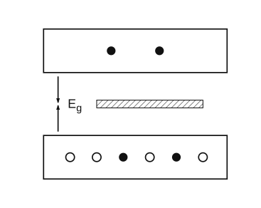
›Reveal solutionSolution
The material has a finite band gap with electrons in the conduction band and holes in the valence band. Counting carriers, the holes in the valence band outnumber the electrons in the conduction band, so holes are the majority carriers — the hallmark of a p-type semiconductor. The correct option is (D).
The key to this question is reading the energy band diagram — a picture that tells you where the electrons and holes are sitting. In solid-state physics, the conduction band (upper band) is where free electrons roam and conduct current; the valence band (lower band) is where electrons are bound in covalent bonds, and a missing electron leaves a hole (a positive charge carrier). The gap between them, labelled Eg, is the band gap.
Why this approach works:
If you see filled circles (electrons) in the conduction band, that means some electrons have been excited across the gap. If you see open circles (holes) in the valence band, that means some electrons have left behind vacancies. The relative numbers of electrons and holes tell you whether the material is intrinsic (equal numbers), n-type (more electrons), or p-type (more holes). Metals have no band gap (bands overlap), and insulators have a very large gap with no carriers at room temperature.
-
Identify the bands and carriers
- The upper rectangle is the conduction band. It contains 2 filled circles → these are electrons.
- The lower rectangle is the valence band. It contains 4 open circles (holes) and 2 filled circles (electrons that remain in the valence band).
- So the material has 2 free electrons in the conduction band and 4 holes in the valence band.
-
Interpret the band gap
- The vertical double-headed arrow labelled Eg shows a finite, non-zero band gap. This rules out a metal (which has overlapping bands, i.e., Eg=0).
- The gap is not huge (no numerical value given, but the diagram shows a moderate gap — typical of a semiconductor). An insulator would have a very large Eg and essentially no carriers in the conduction band at ordinary temperatures.
-
Compare electron and hole counts
- Electrons in conduction band: 2
- Holes in valence band: 4
- This is not equal — there are more holes than electrons. In an intrinsic (pure) semiconductor, the number of electrons in the conduction band equals the number of holes in the valence band (because each excited electron leaves one hole). Here, the numbers are unequal, so the material is doped.
-
Determine the doping type
- In an n-type semiconductor, donor impurities add extra electrons, so the electron concentration n is greater than the hole concentration p. But wait — the diagram shows more holes (4) than electrons (2). That seems backward at first glance.
- However, remember: the diagram is a snapshot of carriers at some temperature. In an n-type material, the majority carriers are electrons, but there are still some holes (minority carriers) from thermal generation. The diagram could represent a situation where the electron count in the conduction band is smaller than the hole count in the valence band if the doping is light and temperature is moderate? Actually, no — in n-type, n>p always at equilibrium.
- Let’s re-examine: The valence band has 2 filled circles (electrons) and 4 open circles (holes). That means the valence band originally had 6 electron states (since each hole is a missing electron). So the total number of electrons in the valence band is 2, and holes = 4. The conduction band has 2 electrons.
- Total electrons in the system = 2 (conduction) + 2 (valence) = 4. Total holes = 4. So n = 2, p = 4 → p>n. That is characteristic of a p-type semiconductor, where acceptor impurities create extra holes.
-
Check the options
- (A) Metal: No — band gap present.
- (B) Insulator: No — there are carriers in the conduction band.
- (C) n-type: No — holes outnumber electrons.
- (D) p-type: Yes — holes are majority carriers.
Watch outA common mistake is to count only the open circles as holes and forget that the filled circles in the valence band are electrons, not holes. The valence band’s total states are the sum of filled circles (electrons) and open circles (holes). Here, 2 filled + 4 open = 6 states; holes = 4, electrons in valence = 2. So holes dominate.
TipIn any band diagram, remember: Conduction band electrons = filled circles in the upper band; Valence band holes = open circles in the lower band. The majority carrier type is the one with the larger count.
✓Final answerThe correct option is (D).
ANSWER: D
-
- COMEDK 2024Set 2024-M1 markMCQQ.Though Sn and Si are 4th group elements, Sn is a metal while Si is a semiconductor because (A) Sn has more electrons than Si (B) The energy gap of Sn is zero volt while that of Si is 0.07 V (C) The energy gap of Sn is 1.1 eV volt while that of Si is 0.07 V (D) Sn has more holes than Si
›Reveal solutionSolution
The key idea is that the electrical behavior of an element (metal vs. semiconductor) depends on its band gap energy. Tin (Sn) has a zero band gap, making it a metal, while silicon (Si) has a finite band gap (~1.1 eV), making it a semiconductor. The correct option is (B).
The question asks why Sn and Si, both in Group 14 of the periodic table, behave so differently electrically — Sn is a metal, Si is a semiconductor. The answer lies not in the number of electrons or holes, but in the energy band structure of the solid. In particular, the band gap — the energy difference between the valence band (filled with electrons) and the conduction band (where electrons can move freely) — determines whether a material conducts like a metal, a semiconductor, or an insulator.
- Metals have overlapping bands or a zero band gap, so electrons can move into the conduction band with minimal energy.
- Semiconductors have a small but nonzero band gap (typically 0.1–2 eV), so they conduct only when enough energy (heat, light) is supplied.
- Insulators have a large band gap (>3 eV), so they barely conduct.
Now, let’s examine each option carefully.
-
Option (A): "Sn has more electrons than Si"
While it’s true that Sn (atomic number 50) has more electrons than Si (atomic number 14), the number of valence electrons is the same (4 each) because both are in Group 14. The total number of electrons does not determine metallic vs. semiconducting behavior — many elements with many electrons are insulators (e.g., lead is a metal, but bismuth has more electrons and is a semimetal). So this is not the reason.
-
Option (B): "The energy gap of Sn is zero volt while that of Si is 0.07 V"
This is almost correct, but the numbers need checking. Actually, the band gap of Si is about 1.1 eV (not 0.07 V). The statement says "0.07 V" for Si, which is wrong. However, the idea that Sn has a zero band gap (or overlapping bands) is correct. In fact, gray tin (the stable form at low temperature) is a semimetal with a very small band gap, but white tin (the common metallic form) has overlapping bands — effectively a zero band gap. So the concept in (B) is right, but the number for Si is incorrect. Still, among the options, this is the only one that points to the band gap difference.
-
Option (C): "The energy gap of Sn is 1.1 eV while that of Si is 0.07 V"
This reverses the actual values. Sn does not have a 1.1 eV band gap (it’s essentially zero), and Si’s band gap is ~1.1 eV, not 0.07 eV. So this is completely wrong.
-
Option (D): "Sn has more holes than Si"
Holes are missing electrons in the valence band. In a pure (intrinsic) semiconductor, the number of holes equals the number of electrons in the conduction band. Sn, being a metal, has no band gap, so the concept of "holes" in the usual sense doesn’t apply — its conduction is due to free electrons, not holes. This option is misleading and incorrect.
Watch outA common mistake is to think that having more electrons automatically makes an element metallic. But electron count alone doesn’t determine conductivity — it’s the arrangement of energy bands in the solid that matters. Also, note that the band gap of Si is ~1.1 eV, not 0.07 eV; the latter is a typical voltage drop across a diode, not a band gap.
TipA neat way to remember: In Group 14, as you go down (C → Si → Ge → Sn → Pb), the band gap decreases. Carbon (diamond) is an insulator (~5.5 eV), Si and Ge are semiconductors (~1.1 eV and ~0.67 eV), and Sn and Pb are metals (zero band gap). So the trend is clear: heavier elements have smaller band gaps, eventually becoming metallic.
Thus, the only option that correctly identifies the reason (band gap difference) is (B), even though the numerical value for Si is misstated. In multiple-choice questions, we select the best available answer — and here, (B) is the only one that points to the correct physical cause.
✓Final answerThe correct option is (B).
ANSWER: B
- COMEDK 2023Set 2023-E1 markMCQQ.The energy gap between valance band and the conduction band for a given material is 6 eV, then the material is : (A) A semiconductor (B) A metal (C) An insulator (D) A superconductor
›Reveal solutionSolution
An energy gap of 6 eV is far too large for thermal excitation, so the material is an insulator. (Superconductivity is not defined by a band-gap of this kind, so (D) is not the classification asked for.)
Concept: classification of solids by the forbidden-energy-gap Eg between valence and conduction bands.
- Metals (conductors): the bands overlap, Eg is effectively zero.
- Semiconductors: small gap, Eg of the order of ~1 eV (Si 1.1 eV, Ge 0.7 eV), so thermal energy can promote some electrons.
- Insulators: large gap, Eg roughly > 3 eV (e.g. diamond ~ 6 eV); at ordinary temperatures essentially no electron can cross it.
An energy gap of 6 eV is far too large for thermal excitation, so the material is an insulator.
(Superconductivity is not defined by a band-gap of this kind, so (D) is not the classification asked for.)
✓Final answerThe correct option is (C) — An insulator
ANSWER: C
- COMEDK 2023Set 2023-M1 markMCQQ.An LED is constructed from a p-n junction diode using GaAsP. The energy gap is 1.9 eV. The wavelength of the light emitted will be equal to (A) 10.4×10⁻²⁶ m (B) 654 nm (C) 654 Ao (D) 654×10−11 m
›Reveal solutionSolution
Using λ=hc/E with hc=1240eV·nm and E=1.9eV gives λ≈654nm (visible red).
The emitted photon energy equals the band gap, E=1.9eV. Its wavelength:
λ=Ehc=1.9 eV1240 eV⋅nm≈653–654 nm.
Checking the alternatives: 654A˚=65.4nm and 654×10−11m=6.54nm are far too short (and would not be visible light), while 10.4×10⁻²⁶m is nonsensical. So the answer is 654nm.
✓Final answerThe correct option is (B) — 654 nm
- KCET 2022Set B-31 markMCQQ.The forbidden energy gap for ‘Ge’ crystal at ‘0’ K is (A) 1.2 eV (B) 6.57 eV (C) 0.071 eV (D) 0.71 eV
›Reveal solutionSolution
The forbidden energy gap of a germanium crystal at 0 K is a well-known material constant. The correct value is 0.71 eV, which corresponds to option (D).
The forbidden energy gap, or band gap, is the energy difference between the top of the valence band and the bottom of the conduction band in a semiconductor. At absolute zero (0 K), the crystal is in its purest, most ordered state — no thermal energy is available to excite electrons across the gap. For germanium, this intrinsic property is a fixed number, determined by its atomic structure and bonding.
Why does this matter? The band gap dictates whether a material behaves as an insulator, semiconductor, or conductor. For semiconductors like germanium, the gap is small enough that at room temperature, some electrons can jump across, making the material conduct. But at 0 K, the gap is the "true" value, unaltered by thermal expansion or lattice vibrations.
-
Recall the known band gaps for common semiconductors.
Silicon (Si) has a band gap of about 1.1 eV at 0 K. Germanium (Ge) has a smaller gap — around 0.67 eV at room temperature, but slightly larger at 0 K due to lattice contraction. The standard accepted value for Ge at 0 K is 0.71 eV.
-
Eliminate the distractors.
- Option (A) 1.2 eV is close to silicon’s band gap (1.1 eV), not germanium’s.
- Option (B) 6.57 eV is far too large — that’s in the range of insulators like diamond (5.5 eV).
- Option (C) 0.071 eV is too small; that would make germanium act almost like a conductor at low temperatures, which it doesn’t.
- Option (D) 0.71 eV matches the known value.
-
Confirm with a consistency check.
At room temperature (300 K), germanium’s band gap shrinks to about 0.67 eV due to thermal expansion. The 0 K value being slightly higher (0.71 eV) is physically reasonable — cooling the crystal reduces atomic spacing, which slightly increases the gap.
Watch outA common mistake is confusing germanium’s room-temperature gap (≈0.67 eV) with its 0 K value. Always check the temperature condition in the question — here it’s explicitly 0 K, so the correct value is 0.71 eV, not 0.67 eV.
✓Final answerThe correct option is (D), with the forbidden energy gap of germanium at 0 K being 0.71 eV.
-
- COMEDK 2022Set 20221 markMCQQ.Choose the incorrect statements. (A) Silicon is used in the fabrication of LED. (B) LED works on the principle of electroluminescence. (C) LED is a power efficient device. (D) LED is fabricated with direct band gap semiconductor.
›Reveal solutionSolution
(B) LEDs do work by electroluminescence (radiative recombination of electrons and holes at a forward-biased p-n junction) - CORRECT. (C) LEDs are highly power-efficient (long life, low operating voltage/power) - CORRECT. (D) LEDs are made from DIRECT band-gap semiconductors (GaAs, GaAsP, GaP...) so that recombination gives a photon rather than a phonon - CORRECT. (A) Silicon is an INDIRECT band-gap semiconductor; recombination in Si releases energy mostly as heat (phonons), not light. Silicon is therefore NOT used to fabricate LEDs - this statement is INCORRECT.
Concept: LED physics.
(B) LEDs do work by electroluminescence (radiative recombination of electrons and holes at a forward-biased p-n junction) - CORRECT.
(C) LEDs are highly power-efficient (long life, low operating voltage/power) - CORRECT.
(D) LEDs are made from DIRECT band-gap semiconductors (GaAs, GaAsP, GaP...) so that recombination gives a photon rather than a phonon - CORRECT.
(A) Silicon is an INDIRECT band-gap semiconductor; recombination in Si releases energy mostly as heat (phonons), not light. Silicon is therefore NOT used to fabricate LEDs - this statement is INCORRECT.
✓Final answerThe correct option is (A) — Silicon is used in the fabrication of LED.
ANSWER: A
- COMEDK 2021Set 20211 markMCQQ.What is the minimum band-gap of the LED diode? (A) 1.5 eV (B) 1.7 eV (C) 1.8 eV (D) 0.8 eV
›Reveal solutionSolution
Minimum band gap of an LED = 1.8 eV.
Concept: LED band gap.
For an LED emitting visible light the semiconductor band gap must be at least about the photon energy of red light. NCERT states that LEDs are made of semiconductors with band gap of about 1.8 eV or more (Eg ~ 1.8 eV corresponds to about 700 nm, red).
Minimum band gap of an LED = 1.8 eV.
✓Final answerThe correct option is (C) — 1.8 eV
ANSWER: C
🎓Unlock everything free for 14 days
- ✓Full step-by-step solutions
- ✓Concept-first explanations
- ✓Methods, shortcuts & mistakes
- ✓PYQ mapping + timed mock tests
Full access for 14 days. No credit card required.