Physics · Ch 16 — Semiconductor Devices
Introduction
Introduction
In Class XI we studied the p-n junction diode's basic switching behaviour: forward biased, it behaves like a closed switch and current flows; reverse biased, it behaves like an open switch and only a negligibly small current flows. This chapter puts that one behaviour to work as the foundation of practical electronics, and then goes well beyond it. Electric power is generated and transmitted as AC because that is more cost-effective at both the generation and transmission stages -- in India, standard mains supply is 230 V at 50 Hz, and it varies sinusoidally with time. Yet a great many everyday electronic devices (a mobile charger, a TV, a laptop adaptor) need a steady DC supply internally. Bridging this gap is the job of a chain of circuits built from diodes: first a RECTIFIER converts the incoming AC voltage into a unidirectional but still pulsating DC voltage; then a FILTER circuit removes most of the leftover AC component (called ripple) riding on that pulsating DC, leaving an almost-steady DC level; and finally, where needed, a VOLTAGE REGULATOR circuit locks the output at exactly the desired DC voltage, holding it steady even if the input voltage or the load current varies. This chapter works through all three stages -- rectifiers (half wave and full wave), filters, and Zener-diode voltage regulation -- and then introduces several other special-purpose junction diodes (photodiode, solar cell, LED) that exploit a semiconductor junction's photosensitivity rather than its rectifying action. The second half of the chapter turns to a genuinely different three-terminal device, the bipolar junction transistor (BJT), covering its structure, biasing, characteristic curves, and its single most important application: amplification. The chapter closes with an introduction to digital electronics and logic gates, the building blocks of all digital circuitry.
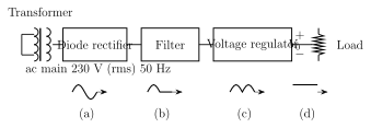
Drawn by us to help you understand the concept clearly, and verified to make sure it's accurate. For exams, practice from your textbook's own diagram.
What this figure shows. A left-to-right block diagram showing the stages a mains AC supply passes through to become clean regulated DC. Stage 1: a step-down TRANSFORMER, primary connected to the 230 V/50 Hz AC mains, secondary feeding stage 2. Alongside stage 1's output, waveform (a) is drawn: a smooth sinusoidal AC wave, symmetric above and below the time axis, labelling the transformer's secondary AC voltage. Stage 2: a RECTIFIER block (a diode or diode arrangement) converting this AC into unidirectional current; waveform (b) drawn at its output is a PULSATING wave -- a series of humps all on the same (positive) side of the time axis, never crossing to negative, but with a clearly varying (rippled) magnitude between humps, not flat. Stage 3: a FILTER block; waveform (c) at its output is a much smoother, nearly flat line sitting well above the axis but still showing a small residual wavy ripple riding on top of the near-constant level, explicitly noted as still containing some ripple. Stage 4: a VOLTAGE REGULATOR block; waveform (d) at its final output is a perfectly flat, constant horizontal line at the desired DC voltage, with no visible ripple at all -- pure DC.
16.1: Fig. 16.1: Block diagram of a simple rectifier/regulated-power-supply chain.