Physics · Ch 16 — Semiconductor Devices
Bipolar Junction Transistor (BJT)
Bipolar Junction Transistor (BJT)
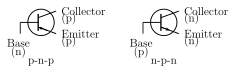
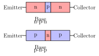
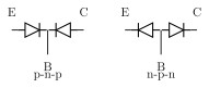
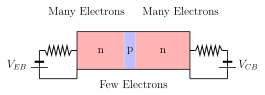
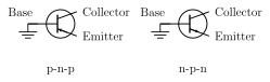
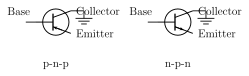
A junction transistor is a semiconductor device having TWO junctions and THREE terminals; because current in it is carried by both electrons and holes together, it is called a BIPOLAR JUNCTION TRANSISTOR (BJT). It consists of three doped regions forming two back-to-back p-n junctions, of which there are two structural types: the n-p-n transistor, formed by growing a thin p-type layer between two relatively thick n-type layers, and the p-n-p transistor, formed by growing a thin n-type layer between two relatively thick p-type layers. The three regions are always named, in order, the EMITTER (E), the BASE (B), and the COLLECTOR (C) -- Fig. 16.18(b). Their circuit symbols (Fig. 16.18a) both draw the emitter lead with an arrowhead: pointing OUTWARD, away from the base, for an n-p-n transistor, and pointing INWARD, towards the base, for a p-n-p transistor -- this arrow direction always indicates the direction of conventional current flow in the emitter. A transistor can be thought of, geometrically, as two p-n junction diodes connected back to back sharing the base as their common middle region (the two-diode analogy, Fig. 16.18c) -- though as the next section makes clear, simply wiring two separate diodes together this way does NOT reproduce genuine transistor action, because the shared base must be a single, extremely thin, lightly-doped region, not two independent junctions.\n\nThe three regions differ deliberately in doping and geometry, and this asymmetry is essential to transistor action: the EMITTER is a thick, HEAVILY doped layer, whose job is to supply a large number of majority carriers into the device; the BASE is thin and LIGHTLY doped (compared to the emitter); and the COLLECTOR is on the far side of the base, also lightly doped -- about ten times more lightly than the base -- and has a LARGER area than either the emitter or the base, so it can collect the majority of the carriers the emitter supplies and also help dissipate any heat generated. Depletion regions form at both junctions (emitter-base and base-collector); because of the differing doping levels, the emitter-base junction has LOW resistance while the base-collector junction has HIGH resistance. In the standard biasing arrangement used for normal ('active region') operation, the emitter-base junction is FORWARD biased and the base-collector junction is REVERSE biased -- this combination is what permits the easy flow of majority carriers from the emitter, all the way through the transistor to the collector.\n\nFor an n-p-n transistor, electrons (the emitter's majority carriers) form the emitter current . The current through the forward-biased E-B junction is large, and -- despite the B-C junction being reverse biased -- the current through it is ALSO large; this seemingly surprising fact is explained by the base's extreme thinness: once the forward bias exceeds the barrier potential (about 0.6-0.7 V for silicon), a large number of electrons are injected from the emitter into the base (Figs. 16.19b-c). Once inside the thin base, these electrons split into two paths (Fig. 16.19d): the great majority diffuse straight across the thin base region and, on reaching the base-collector depletion region, are swept by its field into the collector, forming the COLLECTOR CURRENT (about 95% of ); only a small minority recombine with the base's own (sparse) majority carriers and leave via the base terminal, forming the much smaller BASE CURRENT (about 5% of ). Overall, , and since is so small, to a good approximation. A p-n-p transistor works identically, except that holes (not electrons) are the majority carriers doing the work.\n\nA transistor can be connected into a circuit in three possible …
Drawn by us to help you understand the concept clearly, and verified to make sure it's accurate. For exams, practice from your textbook's own diagram.
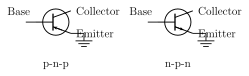
What this figure shows. Two separate transistor symbols shown side by side. Both share the same basic layout: a short vertical base line (B) with two angled leads coming off it -- one to the emitter (E) and one to the collector (C), both terminals drawn touching the base line at an angle (like a 'less-than' or 'greater-than' shape opening towards the base). The EMITTER lead alone carries an ARROWHEAD, and this arrowhead is what distinguishes the two types: for the n-p-n symbol, the arrow on the emitter lead points OUTWARD, AWAY from the base (pointing away from the transistor); for the p-n-p symbol, the arrow on the emitter lead points INWARD, TOWARDS the base. In both symbols the collector lead carries no arrowhead. Each symbol is also labelled with the doping sequence of its three regions in order …
Drawn by us to help you understand the concept clearly, and verified to make sure it's accurate. For exams, practice from your textbook's own diagram.
What this figure shows. A rectangular cross-section divided into three adjoining regions side by side: a WIDE, heavily-shaded region on one end labelled EMITTER (E) and marked n-type, a very THIN middle region labelled BASE (B) and marked p-type, and a WIDE region on the other end labelled COLLECTOR (C) and marked n-type, explicitly drawn with a noticeably LARGER area/width than the emitter region (even though both are labelled 'n', the collector block is drawn visibly bigger than the emitter block to show its larger physical area). Each of the three regions has its own external electrical lead/terminal drawn coming off it (E, B, C respectively), with the base's termi …
Drawn by us to help you understand the concept clearly, and verified to make sure it's accurate. For exams, practice from your textbook's own diagram.
What this figure shows. The same three regions (Emitter, Base, Collector) as Fig. 16.18(b), but redrawn conceptually as TWO SEPARATE p-n junction diodes connected BACK TO BACK, sharing the base region as their common middle terminal: one diode symbol drawn between the emitter and base terminals (the emitter-base junction, E-B), and a second, independent diode symbol drawn between the base and collector terminals (the base-collector junction, B-C), with their orientations mirrored around the shared base -- illustrating that a transistor's two junctions individually behave like two ordinary diodes, even though (as the surrounding text stresses) simply wiring two separate diodes together this way does NOT reproduce true transistor action, because a real transistor's …
Drawn by us to help you understand the concept clearly, and verified to make sure it's accurate. For exams, practice from your textbook's own diagram.
What this figure shows. An n-p-n transistor (E, B, C regions as in Fig. 16.18b) shown with TWO separate DC bias sources connected: a battery connected between the emitter and base terminals with its polarity arranged so the EMITTER-BASE junction is FORWARD biased (emitter's n-region connected to the battery's negative terminal, base's p-region to the positive terminal, marked '-' near emitter side and '+' near base side of this battery), and a second, separate battery connected between the collector and base terminals with its polarity arranged so the COLLECTOR-BASE junction is REVERSE biased (collector's n-region connected to the battery's positive terminal, marked '+' near collector side and '-' near base side of this battery) - …
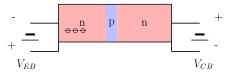
Drawn by us to help you understand the concept clearly, and verified to make sure it's accurate. For exams, practice from your textbook's own diagram.
What this figure shows. The same n-p-n structure and biasing as Fig. 16.19(a), but drawn at the very FIRST INSTANT the forward bias is applied to the E-B junction: a cluster of electrons (marked as '-' symbols, the majority carriers of the n-type emitter) is shown still confined WITHIN the emitter region only, none of them having yet crossed into the base region -- illustrating the 'before' snapshot, immediately preceding the moment (shown in the next figure) when these electrons begin entering the base. …
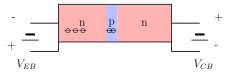
Drawn by us to help you understand the concept clearly, and verified to make sure it's accurate. For exams, practice from your textbook's own diagram.
What this figure shows. The same n-p-n structure and biasing as Figs. 16.19(a)-(b), now drawn once the applied base-emitter voltage exceeds the barrier potential (about 0.6-0.7 V for silicon): a large number of electrons (still marked '-') are now shown having crossed OVER from the emitter region INTO the thin base region, forming the emitter current -- illustrating the 'after' snapshot where majority-carrier injection from emitter into base has begun, the electrons now shown spread across/entering th …
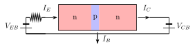
Drawn by us to help you understand the concept clearly, and verified to make sure it's accurate. For exams, practice from your textbook's own diagram.
What this figure shows. The same n-p-n structure, now showing the electrons injected into the thin base region SPLITTING into two separate onward paths, marked with arrows: the great majority of the electrons continue diffusing straight across the thin base and are swept, by the collector-base junction's field, into the collector region, forming the COLLECTOR CURRENT (an arrow shown flowing out through the collector terminal, drawn as clearly the larger/thicker of the two paths, since ); a small minority of the electrons instead recombine with the base's own (sparse) majority holes and flow out through the base terminal, forming the smaller BASE CURRENT (a thinner arrow out through the base terminal, since is only about 5% of ). The emitter current (arrow into the emitter terminal) is shown as the sum/source of both thes …
Drawn by us to help you understand the concept clearly, and verified to make sure it's accurate. For exams, practice from your textbook's own diagram.
What this figure shows. A transistor symbol (E, B, C leads as in Fig. 16.18a) drawn with the INPUT signal applied across the base-emitter terminals (base and emitter forming the input port/loop) and the OUTPUT signal taken across the collector-emitter terminals (collector and emitter forming the output port/loop) -- so the EMITTER terminal is the one lead common to both the input loop and the output loop, which is what gives this confi …
Drawn by us to help you understand the concept clearly, and verified to make sure it's accurate. For exams, practice from your textbook's own diagram.
What this figure shows. The same transistor symbol, now drawn with the INPUT signal applied across the emitter-base terminals and the OUTPUT signal taken across the collector-base terminals -- so the BASE terminal is the one lead common to both the input and output loops in this arrangement, distinguishing it from the common-emitter layout of Fig. 16. …
Drawn by us to help you understand the concept clearly, and verified to make sure it's accurate. For exams, practice from your textbook's own diagram.
What this figure shows. The same transistor symbol, now drawn with the INPUT signal applied across the base-collector terminals and the OUTPUT signal taken across the emitter-collector terminals -- so the COLLECTOR terminal is the one lead common to both the input and output loops in this third and final arrangement, completing the set of three possible single-transistor configurations alongside Figs. 16. …