Q.A sealed box has three terminals A, B and C. Inside, two identical germanium diodes (each with a forward threshold of about 0.7V) and one 1000Ω resistor are connected in some arrangement among the terminals. Using a d.c. source, an ammeter and a voltmeter, the current-voltage (I-V) characteristic is measured between each pair of terminals, with the third terminal left unconnected. The results are:
🔒You're viewing a preview — the full solution, concept, methods & PYQ mapping are locked.
🔒 Start your 14-day free trial to unlock the full solution →Concept understanding — P N Junction Biasing
P-N Junction Biasing: The First Meeting
Imagine you have two rooms separated by a door. One room is full of people who want to leave (electrons in the N-side), and the other room is full of empty chairs (holes in the P-side). The door is initially locked — that's the depletion region, a zone with no free charges. Now, what happens if you push on the door from one side, or pull it from the other? That's exactly what biasing does to a P-N junction.
The Unbiased Junction (The Starting Point)
When you bring P-type and N-type semiconductors together, something interesting happens at the boundary. Electrons from the N-side (which has extra electrons) rush toward the P-side (which has extra holes). Holes from the P-side rush toward the N-side. They meet and recombine — an electron falls into a hole, and both disappear as free charges.
This leaves behind a region near the junction with no free charges — just fixed positive ions on the N-side (where electrons left) and fixed negative ions on the P-side (where holes left). This is the depletion region. It acts like a tiny battery: the N-side is positive relative to the P-side, creating a built-in electric field that stops further diffusion. The voltage across this region is about 0.7 V for silicon, 0.3 V for germanium.
The depletion region is not a physical gap — it's a region depleted of mobile charge carriers. The crystal is still continuous.
Forward Bias: Pushing the Door Open
Connect the positive terminal of a battery to the P-side and the negative terminal to the N-side. This is forward bias.
What happens? The external battery's positive terminal repels holes in the P-side toward the junction. The negative terminal repels electrons in the N-side toward the junction. Both carriers are pushed toward each other — they overcome the built-in electric field. The depletion region shrinks.
When the applied voltage exceeds about 0.7 V (for silicon), the depletion region becomes so thin that carriers can cross freely. A large current flows. The junction is now "on" — like a switch closed.
Never apply forward bias without a current-limiting resistor. The junction has very low resistance once forward-biased, and the current can destroy it instantly.
Reverse Bias: Pulling the Door Shut
Now reverse the battery: positive to N-side, negative to P-side. This is reverse bias.
The positive terminal attracts electrons from the N-side away from the junction. The negative terminal attracts holes from the P-side away from the junction. Both carriers are pulled apart. The depletion region widens.
The built-in electric field is now reinforced by the external field. Only a tiny current flows — the reverse saturation current, caused by thermally generated electron-hole pairs in the depletion region. This current is typically in the nanoampere range and is almost independent of the applied voltage (until breakdown).
The junction is "off" — like a switch open.
In reverse bias, the depletion region acts as an insulator. The junction blocks current flow except for a negligible leakage current.
The Precise Statement
I=IS(enkTqV−1)
This is the Shockley diode equation. Here:
- I = diode current
- IS = reverse saturation current (very small, typically 10−12 to 10−15 A for silicon)
- q = electron charge (1.6×10⁻¹⁹ C)
- V = applied voltage (positive for forward bias, negative for reverse bias)
- n = ideality factor (1 for ideal, 1–2 for real diodes)
- k = Boltzmann constant (1.38×10⁻²³ J/K) …
Why this formula?
Why a PN Junction Biases the Way It Does
A PN junction is not a resistor. Its current-voltage behaviour is fundamentally asymmetric — and that asymmetry comes directly from the physics of the depletion region and the energy barrier it creates.
The Unbiased Junction: A Built-in Barrier
When P-type and N-type semiconductors are joined, holes from the P-side diffuse into the N-side, and electrons from the N-side diffuse into the P-side. This diffusion leaves behind fixed, charged ions: negative acceptor ions on the P-side, positive donor ions on the N-side. These ions create an electric field that opposes further diffusion.
The result is a depletion region — a zone with no free carriers — and a built-in potential V0 across it. This potential acts as an energy barrier that prevents net current flow at equilibrium.
At equilibrium (zero bias), the net current is zero. The diffusion current (due to concentration gradient) is exactly balanced by the drift current (due to the built-in electric field).
Forward Bias: Lowering the Barrier
Apply a positive voltage V to the P-side relative to the N-side. This external voltage opposes the built-in potential. The net barrier becomes:
Vnet=V0−V
The depletion width shrinks. More importantly, the energy barrier for majority carriers (holes from P-side, electrons from N-side) is reduced. A larger number of carriers now have enough energy to cross the junction.
The current that flows is diffusion current — carriers injected across the junction become minority carriers on the other side, where they recombine. The relationship is exponential because the number of carriers with energy above the barrier follows a Boltzmann distribution.
I=I0(eqV/kT−1)
Here I0 is the reverse saturation current (very small), q is the electron charge, k is Boltzmann's constant, and T is absolute temperature.
Why the exponential? The fraction of carriers with enough energy to surmount a barrier of height q(V0−V) is proportional to e−q(V0−V)/kT. At equilibrium (V=0), this gives a current that exactly cancels the drift current. When V>0, the barrier drops, and the net current becomes proportional to eqV/kT.
Reverse Bias: Raising the Barrier
Apply a negative voltage to the P-side relative to the N-side. Now the external voltage adds to the built-in potential:
Vnet=V0+VR
The barrier becomes higher. The depletion region widens. Diffusion of majority carriers is almost completely suppressed. The only current that flows is a tiny reverse saturation current I0, carried by minority carriers (electrons from the P-side, holes from the N-side) that are swept across by the electric field.
This current is essentially constant with voltage because the number of minority carriers is fixed by thermal generation — it does not depend on the barrier height once the barrier is large enough to block majority carriers. …
A-C conducts only at 1.4V=0.7+0.7, i.e. two diode drops, so both the A-arm and the C-arm are diodes and the resistor is the B-arm. It is a Y (star) network about an internal node O. …
The conducting characteristics fix the layout: A-B conducts (at 0.7V, with 1000Ω in series) only when A is negative; B-C conducts (at 0.7V) only when C is positive; and A-C needs 1.4V — two diode drops — to conduct. This is a Y (star) network: a diode from A and a diode from C meet at an internal node O, with the 1000Ω resistor joining B to O.
Reading the characteristics
Each measurement uses only two terminals (the third floats), so current flows through the two internal components linking those terminals.
- A-C needs 1.4V to conduct (vi): 1.4=0.7+0.7, so the A-to-C path contains two diodes in series. Hence both the A-arm and the C-arm are diodes, and the resistor must be on the B-arm.
- A-B (i, ii): blocks when A is +, conducts at 0.7V with inverse-slope 1000Ω when A is −. So the A-arm diode conducts when A is negative (its cathode faces A), and the 1000Ω resistor is in series on the B-arm.
- B-C (iii, iv): blocks when C is −, conducts at 0.7V when C is +. So the C-arm diode conducts when C is positive (its anode faces C), again with the B-arm resistor in series.
- A-C (v, vi): blocks when A is +/C is −; conducts when A is −/C is + at 1.4V — the sum of the two diode drops, with the resistor not in this path.
The arrangement
Introduce an internal node O:
- A-O: a diode with its cathode towards A (conducts when A is negative w.r.t. O).
- C-O: a diode with its anode towards C (conducts when C is positive w.r.t. O).
- B-O: the 1000Ω resistor.
Equivalently, the two germanium diodes are connected in series between A and C, both pointing the same way (anodes towards C), their common point being O, and the 1000Ω resistor runs from B to O.
Consistency check …
Method: Deducing an Unknown Component Layout from Pairwise I-V Measurements
Step 1 -- Use the highest-threshold measurement to count series diodes.
The A-C measurement needs 1.4 V=0.7 V+0.7 V before it conducts -- exactly two diode drops in series, and no resistor drop (the curve rises steeply right after turn-on, not with a 1000Ω-limited slope). This means the A-to-C path contains both diodes in series, with no resistor in that path -- so the resistor must sit on the third arm, from B.
Step 2 -- Use the A-B measurement to fix the A-side diode's orientation.
A-B conducts (at 0.7 V, with a 1000Ω-limited slope matching the resistor) only when A is negative -- so the diode on the A-side has its cathode facing A (it conducts when A is pulled below the internal node).
Step 3 -- Use the B-C measurement to fix the C-side diode's orientation.
B-C conducts (at 0.7 V) only when C is positive -- so the diode on the C-side has its anode facing C.
Step 4 -- Assemble the star (Y) network around an internal node O.
A diode from A to O with cathode at A; a diode from C to O with anode at C; the 1000Ω resistor from B to O. …
Showing the 12 most recent of 23 on this concept.
- TG EAPCET 2026Set eng-2026-05-09-AN1 markMCQQ.If A, B and C represent the power gain, base resistance and collector resistance respectively of a transistor connected in common emitter configuration, then the common emitter current amplification factor is (A) CAB (B) BAC (C) BAC (D) CAB
›Reveal solutionSolution
For a common-emitter transistor, power gain A=β2RBRC=β2BC, so β=CAB.
In a common-emitter amplifier the power gain equals the current gain times the voltage gain:
A=β×AV=β×(βRBRC)=β2RBRC
With base resistance B=RB and collector resistance C=RC: …
- TG EAPCET 2026Set eng-2026-05-10-FN1 markMCQQ.The incorrect statement about a Zener diode is (A) It is heavily doped (B) The depletion region formed in it is very thick (C) The electric field at its junction is extremely high (D) In general, in a circuit it is reverse biased
›Reveal solutionSolution
A Zener diode is a heavily doped, reverse-biased device with a very thin depletion region and an extremely high junction field. The false statement is the one that claims the depletion region is thick.
The key to this question lies in understanding why a Zener diode behaves differently from an ordinary diode. An ordinary p-n junction breaks down (conducts heavily in reverse bias) only at a high voltage, often destructively. A Zener diode is designed to break down at a precisely controlled, low reverse voltage and to survive that breakdown — this is its normal operating mode.
That controlled, low-voltage breakdown is achieved by heavy doping. When both the p and n sides are doped very heavily, the depletion region becomes extremely narrow. Because the same built-in potential now exists across a much smaller distance, the electric field inside the depletion region becomes enormous — easily reaching millions of volts per meter. This intense field is what pulls electrons out of their covalent bonds (Zener breakdown) at a low applied voltage.
Now let's examine each statement.
-
Statement (A): "It is heavily doped"
This is true. Heavy doping is the defining feature that gives the Zener diode its characteristic low breakdown voltage. Without it, the depletion region would be wider and the breakdown voltage would be much higher.
-
Statement (B): "The depletion region formed in it is very thick"
This is false. Heavy doping means there are more charge carriers available to neutralize the fixed ions near the junction. As a result, the depletion region is actually very thin — typically on the order of tens of nanometres. A thick depletion region is a property of a lightly doped diode, not a Zener diode. …
-
- TG EAPCET 2026Set eng-2026-05-11-FN1 markMCQQ.An electron in n-region of a p-n junction diode moves towards the junction with a speed of 5×10⁵ ms−1 and after penetration through the barrier, the electron enters the p-region with a speed of 3×10⁵ ms−1. The barrier potential of the p-n junction is (Mass of electron =9×10⁻³¹ kg and charge of electron =1.6×10⁻¹⁹ C) (A) 0.5 V (B) 0.45 V (C) 0.7 V (D) 0.65 V
›Reveal solutionSolution
The barrier potential is found by equating the loss in kinetic energy of the electron to the gain in electrical potential energy. The result is 0.45 V, so option (B) is correct.
The key idea here is energy conservation. As the electron moves from the n-region to the p-region across the depletion layer, it must climb over the built-in potential barrier. This barrier opposes the motion of electrons from n to p, so the electron loses kinetic energy and gains electrical potential energy. The loss in kinetic energy equals the charge of the electron times the barrier potential.
- Identify the energy change The electron’s speed drops from vi=5×10⁵ m/s to vf=3×10⁵ m/s. Its kinetic energy decreases by
ΔK=21mvi2−21mvf2=21m(vi2−vf2).
- Relate to electrical potential energy The electron gains electrical potential energy eVb (where Vb is the barrier potential) because it moves against the electric field of the junction. By conservation of energy,
21m(vi2−vf2)=eVb.
- Plug in the numbers Mass m=9×10⁻³¹ kg, charge e=1.6×10⁻¹⁹ C.
vi2=(5×10⁵)2=25×1010=2.5×10¹¹,
vf2=(3×10⁵)2=9×1010=0.9×10¹¹,
vi2−vf2=(2.5−0.9)×1011=1.6×10¹¹.
Then
- TG EAPCET 2026Set ap-2026-05-05-FN1 markMCQQ.In common emitter amplifier, when the base to emitter voltage changes by 20 mV, the change in collector current is 3 mA. If the output resistance is 4 kΩ, then the voltage gain of the amplifier is (A) 300 (B) 600 (C) 400 (D) 800
›Reveal solutionSolution
Voltage gain in a CE amplifier is the product of transconductance and output resistance. Here gm=ΔVBEΔIC=150 mS and Ro=4 kΩ, so AV=150×4=600.
The key idea is that in a common emitter amplifier, the voltage gain is determined by how effectively a small change in base-emitter voltage controls the collector current, multiplied by the load it drives. The transconductance gm captures this control — it’s the ratio of change in collector current to change in base-emitter voltage. Once you have gm, the voltage gain is simply AV=gmRo, where Ro is the output resistance (the load seen by the collector current).
Let’s work it through.
- Find the transconductance gm. The definition is gm=ΔVBEΔIC. Given ΔVBE=20 mV=0.02 V and ΔIC=3 mA=0.003 A,
gm=0.020.003=0.15 S=150 mS.
-
Identify the output resistance.
The problem states the output resistance is 4 kΩ=4000 Ω. In a CE amplifier, this is the resistance seen by the collector current — typically RC or RL depending on context. Here it’s given directly.
-
Compute the voltage gain.
For a common emitter amplifier, the voltage gain (magnitude) is
AV=gmRo.
Substituting: …
- TG EAPCET 2025Set eng-2025-05-02-AN1 markMCQQ.1010 electrons enter the emitter of a junction transistor in a time of 0.4 μs. If 5% of the electrons are lost in the base, then the collector current is (A) 3.0 mA (B) 3.2 mA (C) 3.6 mA (D) 3.8 mA
›Reveal solutionSolution
The collector current is found from the number of electrons reaching the collector per second, accounting for the 5% loss in the base. The result is 3.8 mA, so option (D) is correct.
Concept & Intuition
In a bipolar junction transistor, electrons injected from the emitter into the base are mostly swept across to the collector. A small fraction recombine in the base (here 5%), so the collector current is 95% of the emitter current. The emitter current itself is the charge of the electrons entering per unit time. We just need to compute that charge flow and then apply the loss factor.
Step-by-step solution
-
Find the total charge entering the emitter.
Each electron carries charge e=1.6×10⁻¹⁹ C.
Number of electrons = 1010.
Total charge Q=1010×1.6×10−19=1.6×10⁻⁹ C.
-
Compute the emitter current.
Time interval Δt=0.4 μs=0.4×10⁻⁶ s. …
-
- TG EAPCET 2025Set eng-2025-05-02-AN1 markMCQQ.An electron in n-region of a p-n junction moves towards the junction with a speed of 5×10⁵ ms−1. If the barrier potential of the junction is 0.45 V, then the speed with which the electron enters the p-region after penetration through the barrier is (Charge of the electron =1.6×10⁻¹⁹ C and mass of the electron =9×10⁻³¹ kg) (A) 3×10⁵ ms−1 (B) 5×10⁵ ms−1 (C) 4×10⁵ ms−1 (D) 6×10⁵ ms−1
›Reveal solutionSolution
The electron enters the p-region with speed 3×10⁵m/s — option (A).
Given: vi=5×10⁵m/s, barrier potential V=0.45V, e=1.6×10⁻¹⁹C, m=9×10⁻³¹kg.
An electron is a majority carrier in the n-region; the built-in barrier decelerates it as it crosses to the p-region, so it loses kinetic energy eV.
Energy conservation:
21mvf2=21mvi2−eV.
Initial KE:
21mvi2=21(9×10⁻³¹)(5×10⁵)2=1.125×10⁻¹⁹J.
Energy lost: …
- TG EAPCET 2025Set ap-2025-04-30-FN1 markMCQQ.If the breakdown voltage of a Zener diode is 7.2 V and the maximum power dissipated is 216 mW, then the maximum current through the Zener diode is (A) 30 mA (B) 4.16 mA (C) 3.33 mA (D) 2.4 mA
›Reveal solutionSolution
The maximum current through a Zener diode is found by dividing its maximum power dissipation by its Zener breakdown voltage. For the given values, the maximum current is 30 mA.
Concept and Intuition
A Zener diode is a special type of diode designed to operate in the reverse breakdown region. When reverse biased, it maintains a nearly constant voltage across its terminals, known as the Zener voltage (VZ), even as the current through it varies over a wide range. This property makes Zener diodes ideal for voltage regulation.
Every electronic component has a limit to how much power it can dissipate without being damaged. For a Zener diode, this maximum power dissipation (Pmax) is specified by the manufacturer. Power dissipation in any component is given by the product of the voltage across it and the current flowing through it (P=V×I).
In the Zener breakdown region, the voltage across the diode is essentially constant at VZ. Therefore, the power dissipated by the Zener diode is PZ=VZ×IZ, where IZ is the current flowing through the Zener diode. To find the maximum current the Zener diode can safely handle, we use its maximum power dissipation rating and its Zener voltage.
The maximum current (IZ(max)) through a Zener diode is given by:
IZ(max)=VZPmax
where Pmax is the maximum power dissipation and VZ is the Zener breakdown voltage.
Step-by-step Derivation
-
Identify the given parameters:
We are given the Zener breakdown voltage (VZ) and the maximum power dissipated (Pmax).
- Zener breakdown voltage, VZ=7.2 V
- Maximum power dissipated, Pmax=216 mW
-
Convert units to SI base units:
It is good practice to convert all given values to their standard SI units before calculation to avoid errors.
- Pmax=216 mW=216×10−3 W …
-
- TG EAPCET 2025Set ap-2025-04-30-FN1 markMCQQ.For a common emitter transistor amplifier, the voltage across the collector resistance is 2.8 V. If the current amplification factor of the transistor is 70 and the collector resistance is 2 kΩ, then the base current is (A) 20 μA (B) 30 μA (C) 10 μA (D) 40 μA
›Reveal solutionSolution
The collector current is found from the voltage across the collector resistor, then the base current is obtained using the current gain β=70. The base current is 20 μA.
The key idea here is that in a common emitter amplifier, the collector current IC is related to the base current IB by the current amplification factor β (also called hfe). The voltage across the collector resistor RC tells us IC directly via Ohm’s law, and then we simply divide by β to get IB.
- Find the collector current. The voltage across the collector resistance RC=2 kΩ is given as VRC=2.8 V. By Ohm’s law:
IC=RCVRC=2000 Ω2.8 V=0.0014 A=1.4 mA.
- Relate collector current to base current. For a common emitter transistor, the current amplification factor β is defined as:
β=IBIC.
Here β=70, so:
IB=βIC=701.4 mA=0.02 mA=20 μA. …
- TG EAPCET 2024Set ap-2024-05-08-FN1 markMCQQ.The power delivered by the battery shown in the figure is (Take the forward and reverse biased resistances of the diode are zero and infinity respectively) [FIGURE] (A) 2.50 W (B) 5.00 W (C) 7.50 W (D) 3.75 W
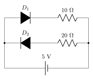
›Reveal solutionSolution
The two diodes face opposite ways, so only one branch conducts — the one with the 10 Ω resistor. The reverse-biased branch is an open circuit, so P=V2/R=52/10=2.50 W — option (A).
The concept first
An ideal diode is nothing more mysterious than a switch controlled by the direction of the applied voltage:
- Forward biased (p-side at higher potential): the depletion layer collapses, resistance →0 — treat it as a short circuit / piece of wire.
- Reverse biased (p-side at lower potential): the depletion layer widens, resistance →∞ — treat it as an open circuit / broken wire. A branch containing a reverse-biased ideal diode can simply be rubbed out of the circuit diagram.
That is the whole trick of these problems: redraw the circuit with the reverse-biased branches deleted and the forward-biased diodes replaced by wires. What is left is a plain resistor network.
Here, the two branches hang across the same pair of nodes (they are in parallel) and therefore see the same voltage with the same polarity. But D1 and D2 are drawn pointing in opposite directions. Conventional current can pass through a diode only in the direction of its arrowhead. So for whichever way round the battery is connected, exactly one diode is forward biased and the other is reverse biased — the two can never conduct together. One branch lives; the other is dead.
Step-by-step
- Identify the conducting branch. With the battery polarity as drawn, the branch whose diode arrow points along the direction the battery drives current is forward biased. That is the D1 + 10 Ω branch. D2, pointing the opposite way, is reverse biased.
- Apply the ideal-diode model.
- D1: forward biased ⇒ RD1=0 ⇒ replace by a wire. The branch is just 10 Ω. …
- TG EAPCET 2023Set eng-2023-05-12-AN1 markMCQQ.The magnetic susceptibility of ferromagnetic materials is (A) <0 (B) >1 (C) 1 (D) 0
›Reveal solutionSolution
Ferromagnetic materials have a very large positive magnetic susceptibility (much greater than 1) due to spontaneous alignment of magnetic domains. The correct option is (B).
Concept & Intuition
Magnetic susceptibility (χ) measures how easily a material becomes magnetized in an external magnetic field. For ferromagnetic materials (like iron, nickel, cobalt), the internal atomic magnetic moments align strongly and cooperatively, producing a huge magnetization even in a weak field. This is fundamentally different from paramagnetic materials (small positive χ, typically 10−5 to 10−3) or diamagnetic materials (small negative χ, about −10−5). Ferromagnets have χ values ranging from 102 to 106 — always positive and much greater than 1.
Step-by-step reasoning
-
Recall the definition of magnetic susceptibility
The magnetic susceptibility χ is defined by M=χH, where M is magnetization and H is the applied magnetic field. For linear materials, χ is a constant; for ferromagnets, it is nonlinear but always large and positive.
-
Compare with other magnetic behaviors
- Diamagnetic materials: χ<0 (small negative, e.g., copper, water).
- Paramagnetic materials: 0<χ≪1 (small positive, e.g., aluminum, oxygen).
- Ferromagnetic materials: χ≫1 (large positive, e.g., iron has χ≈200 at room temperature).
-
Eliminate incorrect options
- Option (A) <0: This describes diamagnetism, not ferromagnetism.
- Option (C) 1: This would mean the material is exactly as magnetizable as a vacuum (relative permeability μr=2), which is not true for any ferromagnet. …
-
- TG EAPCET 2023Set eng-2023-05-13-FN1 markMCQQ.The built-in potential of a p-n junction diode is 0.7V. If the diode is forward biased and the applied voltage is 0.3V, the effective barrier height is (A) 0.7V (B) 0.3V (C) 0.4V (D) 1V
›Reveal solutionSolution
The effective barrier height in a forward-biased p-n junction is the built-in potential minus the applied forward voltage, so 0.7V−0.3V=0.4V.
The key idea is that a p-n junction has a built-in potential barrier (here 0.7V) that opposes the flow of majority carriers. When we apply a forward bias (positive voltage to p-side, negative to n-side), we are essentially pushing carriers toward the junction, which lowers the barrier. The effective barrier height is therefore the original built-in potential reduced by the applied voltage.
Why subtract?
Think of the built-in potential as a hill that carriers must climb. Forward bias is like an external push that helps them up the hill — it effectively reduces the hill’s height. So the net height they face is the original hill minus the push.
Now, step by step:
-
Identify the built-in potential
Given: Vbi=0.7V. This is the barrier with no external voltage.
-
Identify the applied forward bias
Given: Vapplied=0.3V (forward bias means the p-side is positive relative to the n-side).
-
Determine the effective barrier
In forward bias, the effective barrier height is:
Veff=Vbi−Vapplied
Substitute:
Veff=0.7V−0.3V=0.4V …
-
- TG EAPCET 2023Set eng-2023-05-14-AN1 markMCQQ.When an n-type semiconductor is heated (A) number of electrons increases while that of holes decreases (B) number of holes increases while that of electrons decreases (C) number of holes and electrons do not change (D) number of holes and electrons increases equally
›Reveal solutionSolution
In an n-type semiconductor, heating generates equal numbers of electron-hole pairs, so both carrier concentrations increase equally — the correct answer is (D).
Concept and Intuition
An n-type semiconductor is doped with donor atoms that provide extra electrons, making electrons the majority carriers and holes the minority carriers at room temperature. When you heat it, you're not just affecting the dopants — you're also providing enough thermal energy to break covalent bonds in the semiconductor lattice itself. Each broken bond creates one free electron and one hole (an electron-hole pair). This intrinsic generation happens equally for both carriers, regardless of the doping type. So while the original majority/minority imbalance remains, both populations rise by the same amount.
Step-by-Step Reasoning
-
Understand the initial state
At room temperature, an n-type semiconductor has many free electrons from donor atoms (e.g., phosphorus in silicon) and relatively few holes. The electron concentration n≈ND (donor density), and the hole concentration p≈ni2/ND, where ni is the intrinsic carrier concentration.
-
What happens when temperature increases?
Heating provides energy that can break covalent bonds in the semiconductor. Each broken bond generates one electron and one hole — this is called intrinsic carrier generation. The number of such pairs increases with temperature.
-
Effect on electrons and holes
- Electrons: The original donor electrons are still there, plus the newly generated electrons from bond breaking. So the total electron concentration increases.
- Holes: The original few holes are still there, plus the newly generated holes from bond breaking. So the hole concentration also increases.
-
Are the increases equal? …
-
🎓Unlock everything free for 14 days
- ✓Full step-by-step solutions
- ✓Concept-first explanations
- ✓Methods, shortcuts & mistakes
- ✓PYQ mapping + timed mock tests
Full access for 14 days. No credit card required.