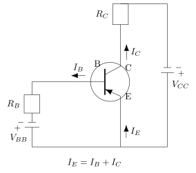
Transistor Action — The Intuition First
Imagine a narrow hallway with a door at each end. The first door (emitter-base junction) is wide open — people can pour in easily. The second door (collector-base junction) is almost closed, but it opens inward only, so once someone passes through the hallway they can leave but cannot come back. The hallway itself is very short and thin (the base). Most people who enter through the first door will walk straight through and exit the second door, because the hallway is too narrow for them to linger or turn around.
That is the core picture of a bipolar junction transistor (BJT) in active mode.
The emitter is heavily doped — it has a huge supply of charge carriers (electrons for an n-p-n, holes for a p-n-p). The base is very thin and lightly doped. The collector is moderately doped and physically large. When you forward-bias the emitter-base junction, carriers flood from the emitter into the base. Once inside the base, these carriers are minority carriers — they are not supposed to be there. The base region is so thin that most of them diffuse across it before they have a chance to recombine with majority carriers. When they reach the collector-base junction, the reverse bias there sweeps them into the collector because the electric field of the depletion region pulls them across.
That is transistor action: a small current in the emitter-base loop controls a much larger current in the collector-base loop, because nearly all the injected carriers make it to the collector.
The Precise Statement
Transistor action is the phenomenon in which, under active-mode biasing (EB junction forward biased, CB junction reverse biased), the majority of charge carriers injected from the emitter into the base diffuse across the thin base region and are collected by the reverse-biased collector-base junction, producing a collector current that is nearly equal to the emitter current.
Mathematically, the collector current IC is related to the emitter current IE by the common-base current gain α:
IC=αIE
where α is typically 0.95 to 0.999. The small fraction that is lost — carriers that recombine in the base or are injected back into the emitter — constitutes the base current IB:
IE=IB+IC
The more familiar common-emitter current gain β is defined as:
β=IBIC=1−αα
A typical β of 100 means that a base current of 10 μA can control a collector current of 1 mA — that is the amplification.
Why It Works — The Three Conditions
-
Emitter heavily doped — ensures a huge supply of carriers to inject. The emitter current is almost entirely due to these injected carriers, not due to majority carriers from the base.
-
Base very thin (≪ diffusion length) — injected carriers reach the collector before they recombine. The base width WB is much smaller than the minority-carrier diffusion length Ln (for n-p-n). Recombination loss is minimal.
-
Collector reverse biased — the strong electric field at the CB junction pulls carriers across, preventing them from accumulating at the base-collector boundary. It also prevents injection of carriers from collector into base. …