Q.i) Why is the base of a transistor made very thin and lightly doped? ii) Draw a circuit diagram of an n-p-n transistor in CE configuration. iii) Evaluate: a) 1000[?] + 1111 b) 1100·101 – 1001·11
You're viewing a preview — the full solution, concept, methods & PYQ mapping are locked.
Start your 14-day free trial to unlock the full solution →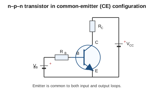
(i) A thin, lightly-doped base minimises recombination so nearly all emitter carriers reach the collector, giving good current gain. (ii) n-p-n CE: emitter-base forward biased, collector-base reverse biased, base common. (iii)(a) the first operand's last bit is watermark-hidden, so the sum is 11111 or 100000 (cannot confirm); (iii)(b) 1100.101 - 1001.11 = 10.111.
(i) Why the base is thin and lightly doped: The emitter injects a large number of majority carriers into the base. If the base is very thin and only lightly doped, there are few opposite carriers in the base for them to recombine with, so only a tiny fraction recombines (giving a small base current) and almost all the injected carriers diffuse across to the collector. This makes the collector current nearly equal to the emitter current and gives a large current amplification factor (beta), which is essential for the transistor to work as an efficient amplifier.
(ii) n-p-n transistor in common-emitter (CE) configuration (describe/draw): The emitter (n) is connected so that the emitter-base junction is FORWARD biased (base positive with respect to emitter through a battery VBB and base resistor RB); the collector (n) is connected so that the collector-base junction is REVERSE biased (collector positive through supply VCC and load resistor RC). The EMITTER terminal is common to both the input (base-emitter) loop and the output (collector-emitter) loop. Input signal is applied between base and emitter; output is taken between collector and emitter. Arrow on the emitter points OUTWARD (away from the base) for an n-p-n transistor.
(iii) Binary arithmetic:
(a) 1000? + 1111 - HONESTY (partial data): the fifth (last) digit of the first operand lies under the diagonal watermark and cannot be read with certainty. So there are two possibilities and the exact answer cannot be confirmed:
- If the operand is 10000 (= 16 in decimal): 10000 + 1111 = 11111 (= 16 + 15 = 31). …
Unlock everything free for 14 days
- Full step-by-step solutions
- Concept-first explanations
- Methods, shortcuts & mistakes
- PYQ mapping + timed mock tests
Full access for 14 days. No credit card required.