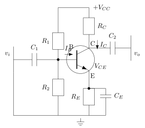
Transistor as an Amplifier
Think of a transistor amplifier like a seesaw where you push down gently on one end and the other end swings up hard. Except here, the "push" is a tiny voltage change at the input, and the "swing" is a large voltage change at the output. The transistor itself is just a valve — it controls a big current using a small signal.
The Core Intuition
A transistor in common-emitter configuration has three terminals: base, emitter, and collector. The base-emitter junction behaves like a diode. A small change in base-emitter voltage (ΔVBE) causes a much larger change in collector current (ΔIC). This is the transistor's transconductance — the ratio ΔIC/ΔVBE, denoted gm.
Now, if you place a resistor RC in the collector path, that changing current produces a changing voltage across RC: ΔVout=−ΔIC⋅RC. The minus sign appears because when collector current increases, the voltage drop across RC increases, pulling the collector voltage down — so the output is inverted relative to the input.
The voltage gain is therefore:
Av=ΔVinΔVout=−gmRC
The gain is simply transconductance times load resistance. A bigger RC gives more gain, but too large a resistor starves the transistor of operating current — there's always a trade-off.
The Precise Statement
A common-emitter transistor amplifier takes a small input voltage signal applied between base and emitter, and produces a larger (but inverted) output voltage signal between collector and emitter. The amplification relies on two things:
-
Transconductance (gm): The transistor converts a voltage change at the input into a current change at the output. For a bipolar junction transistor (BJT) in active region, gm=IC/VT, where VT≈25 mV at room temperature and IC is the quiescent collector current.
-
Load resistor (RC): This resistor converts the current change back into a voltage change. The output voltage swing is −ΔIC⋅RC.
The overall voltage gain is:
Av=−VTIC⋅RC
The gain formula assumes the transistor stays in the active region throughout the signal swing. If the output tries to swing below about 0.2 V (saturation) or above the supply voltage (cutoff), the transistor stops amplifying and the signal distorts.
Why It Works (Step by Step)
- A small increase in VBE (say +5 mV) causes a large increase in IC (because the base-emitter diode is exponential in nature).
- This larger IC flows through RC, increasing the voltage drop across it.
- Since the collector is connected to the supply through RC, the collector voltage drops by the same amount.
- The result: a small positive input produces a large negative output — amplification with inversion.
The transistor does not create energy. The amplified output signal gets its power from the DC supply (VCC). The transistor merely modulates this DC power in proportion to the small input signal. That's why it's called an amplifier, not an energy source.
A Concrete Example …