Q.(a) With the help of a labelled circuit diagram, explain the working of n-p-n transistor as an amplifier in common emitter configuration. [2]
You're viewing a preview — the full solution, concept, methods & PYQ mapping are locked.
Start your 14-day free trial to unlock the full solution →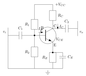
The common-emitter amplifier converts a small base-current swing into a large collector-current swing across a load resistor; because that swing subtracts from the supply voltage, the output moves opposite to the input, giving a 180° phase reversal.
(a) Working of an n-p-n CE amplifier:
Circuit: The emitter is common to both the input (base-emitter) and output (collector-emitter) circuits. The base-emitter junction is forward biased (via and battery , or a potential-divider bias) and the base-collector junction is reverse biased (via and load resistor in the collector circuit). The AC input signal is applied (through a coupling capacitor) across the base-emitter circuit, and the amplified output is taken across the collector resistor (i.e. as the varying ), again via a coupling capacitor.
Working: A small variation in the input signal voltage changes the base current slightly. Because (with , the current-amplification factor in CE mode), this small change in produces a MUCH LARGER change in collector current . This larger flows through the collector load resistor , producing a correspondingly large variation in the voltage drop , and hence a large variation in the output voltage . Thus a small input voltage signal is converted into a much larger output voltage signal — voltage (and power) amplification.
…
Unlock everything free for 14 days
- Full step-by-step solutions
- Concept-first explanations
- Methods, shortcuts & mistakes
- PYQ mapping + timed mock tests
Full access for 14 days. No credit card required.