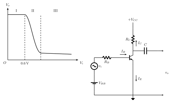
Q.The transfer characteristic of n-p-n transistor in CE configuration is shown in the figure.
You're viewing a preview — the full solution, concept, methods & PYQ mapping are locked.
Start your 14-day free trial to unlock the full solution →Region I (flat, high ) is cut-off, Region II (steep fall) is active, Region III (flat, low ) is saturation; the transistor is off in cut-off; the calculated base signal current is A; and the EB/CB bias combination is what lets the transistor amplify.
(a) Identifying the regions: In the transfer characteristic ( vs ) of an n-p-n CE transistor:
- Region I (for small , below about 0.6 V): the transistor is not conducting, base current is essentially zero, so collector current and (output stays high and flat). This is the cut-off region.
- Region II (the steep, roughly linear falling part of the curve): small changes in produce large changes in , , and hence — the transistor works as a linear amplifier here. This is the active region.
- Region III (for larger , where flattens out at a low value): has reached its maximum possible value (limited by and ) and no longer increases with ; stays low and flat. This is the saturation region.
(b) Region where the transistor is 'switched off': In the cut-off region (Region I) — here and , so essentially no current flows through the transistor, exactly like an open switch.
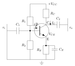
(c) Base signal current: The AC output (signal) voltage across is V, and . The corresponding change in collector current is
The current amplification factor is , so the base signal current is
…
Unlock everything free for 14 days
- Full step-by-step solutions
- Concept-first explanations
- Methods, shortcuts & mistakes
- PYQ mapping + timed mock tests
Full access for 14 days. No credit card required.