Q.Biasing is provided for maintaining proper current flow across a p-n junction.
You're viewing a preview — the full solution, concept, methods & PYQ mapping are locked.
Start your 14-day free trial to unlock the full solution →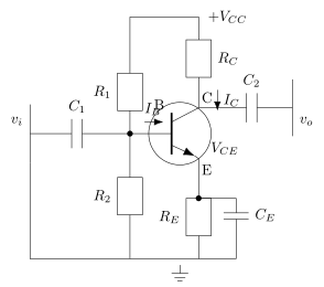
(a) Reverse bias drives minority-carrier holes from n to p. (b) Two oppositely-oriented diodes in parallel branches conduct on both polarities, with different slopes (1/10Ω and 1/20Ω) set by which diode is forward biased. (c) A transistor amplifies current in common-emitter mode because β = ΔIC/ΔIB is large — a thin, lightly-doped base lets nearly all injected carriers reach the collector.
(a) Direction of hole flow
In forward bias, the majority carriers dominate: holes (majority carriers in p) flow from p to n, and electrons (majority in n) flow from n to p — this is the large forward current. The net flow of holes from n to p instead describes the small minority-carrier motion: in the n-region, a few holes exist as minority carriers, and under a bias that widens the depletion region, the internal field sweeps them across to the p-side. This minority-carrier drift happens under reverse bias.
Answer: reverse biased.
(b) V-I characteristic of the two back-to-back branches
Between A and B there are two diodes wired in opposite senses, one with a 10Ω series resistor, the other with a 20Ω series resistor. For any one polarity of the applied voltage across A-B, only one of the two diodes is forward biased (the other is reverse biased and effectively blocks, drawing negligible current):
- For voltage in one direction, the upper diode conducts: current flows through the 10Ω branch once the forward threshold (~0.7 V for Si / ~0.3 V for Ge) is crossed, and the current then rises roughly as .
- For the opposite polarity, the lower diode conducts instead, through the 20Ω branch: .
So, unlike a single diode (which conducts in only one direction), this back-to-back combination conducts current for either polarity of applied voltage, but with a steeper rise (lower resistance, 10Ω) on one side and a gentler rise (higher resistance, 20Ω) on the other — an odd/antisymmetric V-I curve, each branch beginning only after its own turn-on voltage is exceeded.
(c) Transistor as a current amplifier
…
Unlock everything free for 14 days
- Full step-by-step solutions
- Concept-first explanations
- Methods, shortcuts & mistakes
- PYQ mapping + timed mock tests
Full access for 14 days. No credit card required.