Q.[The following is a choice question. Answer any one.]
(A) Draw the circuit diagram of transistor as an amplifier in common emitter configuration. (Scores : 2)
(B) Obtain the expression for the voltage gain. (Scores : 2)
OR
(A) What do you mean by barrier potential of a diode ? (Score : 1)
(B) With the help of a diagram explain the working of a full wave rectifier. (Scores : 3)
You're viewing a preview — the full solution, concept, methods & PYQ mapping are locked.
Start your 14-day free trial to unlock the full solution →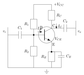
This is an internal-choice question; both options are worked below. A common-emitter amplifier gives voltage gain Av = β_ac(RC/ri); a full-wave rectifier uses two diodes (or a bridge) to conduct current through the load on both halves of the AC cycle.
Option (A) — CE Amplifier
(A) Circuit: an NPN transistor is used with the emitter common to both the input and output loops (grounded, usually via a bypassed emitter resistor RE for bias stability). The base is biased through resistors from VCC (or VBB) to set the quiescent operating point; the AC input signal is coupled to the base via a capacitor. The collector is connected to VCC through a load resistor RC, and the output is taken across RC via another coupling capacitor.
(B) Voltage gain: A small change in base current ΔIB causes a change in collector current ΔIC = β_ac·ΔIB (β_ac = AC current gain of the transistor). This produces a change in the voltage across RC, and hence at the output (collector), of magnitude ΔV0 = ΔIC·RC (with a phase reversal — CE is an inverting amplifier). The input voltage change is ΔVi = ΔIB·ri, where ri is the input resistance of the transistor (base-emitter junction). The voltage gain is:
Av = ΔV0/ΔVi = (ΔIC·RC)/(ΔIB·ri) = β_ac (RC/ri)
Option (B) — Diode barrier potential & full-wave rectifier (OR)
(A) When a p–n junction is formed, majority carriers (electrons from the n-side, holes from the p-side) diffuse across the junction and recombine, leaving behind fixed, uncompensated ions — positive ions on the n-side, negative ions on the p-side — near the junction. This creates a narrow depletion region with an internal electric field pointing from n to p, which opposes further diffusion of majority carriers. The potential difference associated with this internal field is the barrier potential (≈0.7 V for silicon, ≈0.3 V for germanium); an external forward bias must exceed this before appreciable current flows.
…
Unlock everything free for 14 days
- Full step-by-step solutions
- Concept-first explanations
- Methods, shortcuts & mistakes
- PYQ mapping + timed mock tests
Full access for 14 days. No credit card required.