Q.What is a P-N junction diode? With a neat circuit diagram, describe the operation of a full-wave rectifier using junction diodes. (1+6=7)
You're viewing a preview — the full solution, concept, methods & PYQ mapping are locked.
Start your 14-day free trial to unlock the full solution →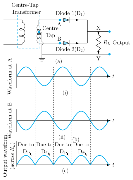
A P-N junction diode conducts in forward bias and blocks in reverse bias; a full-wave rectifier uses diodes to convert both half-cycles of an AC input into a single-direction (pulsating DC) output.
P-N junction diode: A P-N junction diode is formed by joining a P-type semiconductor (majority carriers: holes) and an N-type semiconductor (majority carriers: electrons) together, typically by doping a single crystal of silicon or germanium differently on the two sides. Near the junction, electrons from the N-side diffuse into the P-side and holes from the P-side diffuse into the N-side, leaving behind fixed ions and creating a narrow charge-depleted region called the depletion layer, along with a built-in potential barrier.
In forward bias (P-side connected to the positive terminal, N-side to the negative terminal of a battery), the depletion layer narrows and the diode conducts significant current once the applied voltage exceeds the barrier potential (~0.7 V for silicon). In reverse bias (P-side negative, N-side positive), the depletion layer widens and only a negligible reverse saturation (leakage) current flows — the diode acts essentially as an open switch. This one-way conduction property makes the diode useful as a rectifier.
Full-wave rectifier — operation with a circuit diagram (described in words):
Centre-tapped transformer type: A step-down transformer with a centre-tapped secondary winding is used. The two ends of the secondary winding are each connected, through a diode ( and respectively), to one end of the load resistor ; the other end of is connected to the centre tap of the transformer.
During one half-cycle of the AC input, the end connected to is positive, so conducts (forward biased) while is reverse biased (does not conduct); current flows through and . During the next half-cycle, the polarity reverses: now conducts while is reverse biased, and current again flows through in the same direction as before (because of how the diodes and centre tap are arranged).
…
Unlock everything free for 14 days
- Full step-by-step solutions
- Concept-first explanations
- Methods, shortcuts & mistakes
- PYQ mapping + timed mock tests
Full access for 14 days. No credit card required.