Q.A forward biased diode is treated as
Concept understanding — P N Junction Biasing
P-N Junction Biasing: The First Meeting
Imagine you have two rooms separated by a door. One room is full of people who want to leave (electrons in the N-side), and the other room is full of empty chairs (holes in the P-side). The door is initially locked — that's the depletion region, a zone with no free charges. Now, what happens if you push on the door from one side, or pull it from the other? That's exactly what biasing does to a P-N junction.
The Unbiased Junction (The Starting Point)
When you bring P-type and N-type semiconductors together, something interesting happens at the boundary. Electrons from the N-side (which has extra electrons) rush toward the P-side (which has extra holes). Holes from the P-side rush toward the N-side. They meet and recombine — an electron falls into a hole, and both disappear as free charges.
This leaves behind a region near the junction with no free charges — just fixed positive ions on the N-side (where electrons left) and fixed negative ions on the P-side (where holes left). This is the depletion region. It acts like a tiny battery: the N-side is positive relative to the P-side, creating a built-in electric field that stops further diffusion. The voltage across this region is about 0.7 V for silicon, 0.3 V for germanium.
The depletion region is not a physical gap — it's a region depleted of mobile charge carriers. The crystal is still continuous.
Forward Bias: Pushing the Door Open
Connect the positive terminal of a battery to the P-side and the negative terminal to the N-side. This is forward bias.
What happens? The external battery's positive terminal repels holes in the P-side toward the junction. The negative terminal repels electrons in the N-side toward the junction. Both carriers are pushed toward each other — they overcome the built-in electric field. The depletion region shrinks.
When the applied voltage exceeds about 0.7 V (for silicon), the depletion region becomes so thin that carriers can cross freely. A large current flows. The junction is now "on" — like a switch closed.
Never apply forward bias without a current-limiting resistor. The junction has very low resistance once forward-biased, and the current can destroy it instantly.
Reverse Bias: Pulling the Door Shut
Now reverse the battery: positive to N-side, negative to P-side. This is reverse bias.
The positive terminal attracts electrons from the N-side away from the junction. The negative terminal attracts holes from the P-side away from the junction. Both carriers are pulled apart. The depletion region widens.
The built-in electric field is now reinforced by the external field. Only a tiny current flows — the reverse saturation current, caused by thermally generated electron-hole pairs in the depletion region. This current is typically in the nanoampere range and is almost independent of the applied voltage (until breakdown).
The junction is "off" — like a switch open.
In reverse bias, the depletion region acts as an insulator. The junction blocks current flow except for a negligible leakage current.
The Precise Statement
I=IS(enkTqV−1)
This is the Shockley diode equation. Here:
- I = diode current
- IS = reverse saturation current (very small, typically 10−12 to 10−15 A for silicon)
- q = electron charge (1.6×10⁻¹⁹ C)
- V = applied voltage (positive for forward bias, negative for reverse bias)
- n = ideality factor (1 for ideal, 1–2 for real diodes)
- k = Boltzmann constant (1.38×10⁻²³ J/K)
- T = absolute temperature (K)
For forward bias (V>0), the exponential term dominates — current grows rapidly. For reverse bias (V<0), the exponential term becomes negligible, and I≈−IS — a tiny constant current.
Summary Table
| Condition | Bias | Depletion Region | Current |
|---|---|---|---|
| No external voltage | Unbiased | Moderate width | Zero net current |
| P positive, N negative | Forward bias | Shrinks | Large (exponential) |
| P negative, N positive | Reverse bias | Widens | Tiny (saturation) |
Why This Matters
Every diode, LED, solar cell, and transistor relies on this principle. A solar cell is just a P-N junction under forward bias from light. A transistor uses two junctions back-to-back. The ability to control current flow with a voltage — to switch between "on" and "off" — is the foundation of all modern electronics.
Remember the mnemonic: Positive to P-side = Forward bias (current flows). Negative to P-side = Reverse bias (current blocked). The arrow in the diode symbol points from P to N — the direction of conventional current when forward-biased.
Forward and reverse biasing of the p-n junction, along with the Shockley diode equation, is a core numerical and conceptual topic in the NCERT Class 12 Physics Semiconductor Electronics chapter, frequently searched as "p-n junction biasing important questions" by CBSE board and JEE Main aspirants. This concept is also essential groundwork for understanding rectifiers and transistor circuits covered later in the same syllabus.
Why this formula?
Why a PN Junction Biases the Way It Does
A PN junction is not a resistor. Its current-voltage behaviour is fundamentally asymmetric — and that asymmetry comes directly from the physics of the depletion region and the energy barrier it creates.
The Unbiased Junction: A Built-in Barrier
When P-type and N-type semiconductors are joined, holes from the P-side diffuse into the N-side, and electrons from the N-side diffuse into the P-side. This diffusion leaves behind fixed, charged ions: negative acceptor ions on the P-side, positive donor ions on the N-side. These ions create an electric field that opposes further diffusion.
The result is a depletion region — a zone with no free carriers — and a built-in potential V0 across it. This potential acts as an energy barrier that prevents net current flow at equilibrium.
At equilibrium (zero bias), the net current is zero. The diffusion current (due to concentration gradient) is exactly balanced by the drift current (due to the built-in electric field).
Forward Bias: Lowering the Barrier
Apply a positive voltage V to the P-side relative to the N-side. This external voltage opposes the built-in potential. The net barrier becomes:
Vnet=V0−V
The depletion width shrinks. More importantly, the energy barrier for majority carriers (holes from P-side, electrons from N-side) is reduced. A larger number of carriers now have enough energy to cross the junction.
The current that flows is diffusion current — carriers injected across the junction become minority carriers on the other side, where they recombine. The relationship is exponential because the number of carriers with energy above the barrier follows a Boltzmann distribution.
I=I0(eqV/kT−1)
Here I0 is the reverse saturation current (very small), q is the electron charge, k is Boltzmann's constant, and T is absolute temperature.
Why the exponential? The fraction of carriers with enough energy to surmount a barrier of height q(V0−V) is proportional to e−q(V0−V)/kT. At equilibrium (V=0), this gives a current that exactly cancels the drift current. When V>0, the barrier drops, and the net current becomes proportional to eqV/kT.
Reverse Bias: Raising the Barrier
Apply a negative voltage to the P-side relative to the N-side. Now the external voltage adds to the built-in potential:
Vnet=V0+VR
The barrier becomes higher. The depletion region widens. Diffusion of majority carriers is almost completely suppressed. The only current that flows is a tiny reverse saturation current I0, carried by minority carriers (electrons from the P-side, holes from the N-side) that are swept across by the electric field.
This current is essentially constant with voltage because the number of minority carriers is fixed by thermal generation — it does not depend on the barrier height once the barrier is large enough to block majority carriers.
The reverse current is not zero — it is very small (nanoamps to microamps for silicon) but present. It doubles roughly every 10°C rise in temperature because thermal generation of minority carriers increases.
The Complete Picture: The Diode Equation
The single equation that captures both forward and reverse behaviour is:
I=I0(eqV/nkT−1)
where n is the ideality factor (typically 1 for ideal diodes, 1–2 for real diodes).
- Forward bias (V>0): The exponential term dominates, current grows rapidly.
- Reverse bias (V<0): The exponential term vanishes, I≈−I0 (a small constant).
- At V=0: I=0 — the equation correctly gives zero net current.
For quick calculations at room temperature (300 K), remember qkT≈0.026 V. So eV/0.026 gives the factor by which current increases for every 26 mV of forward bias — a handy rule of thumb.
Why Not Ohm's Law?
A PN junction does not obey Ohm's law because the number of carriers available to conduct current is not constant — it depends exponentially on the applied voltage. The junction is a non-linear device: its resistance changes dramatically with bias direction and magnitude.
In forward bias, the resistance is low and decreases as voltage increases. In reverse bias, the resistance is extremely high (megohms) until breakdown occurs.
This asymmetry — the ability to conduct in one direction and block in the other — is the fundamental reason the PN junction is the building block of almost all semiconductor devices.
A forward-biased diode is not a perfect 0 V short; it is best modelled as a small series resistance in series with a small battery representing its knee voltage.
(d) A closed switch in series with a small resistance and a battery.
Step 1. A truly IDEAL diode (barrier potential and forward resistance both neglected) is a closed switch with 0 V drop -- but that is a simplification, not the most complete model.
Step 2. A REAL forward-biased diode has both a small forward resistance rf=ΔV/ΔI (from the exponential I-V curve) and a knee/threshold voltage (about 0.7 V for silicon) that must be crossed before it conducts appreciably.
Step 3. The most complete equivalent-circuit model therefore combines a small battery (the threshold voltage) with a small series resistance -- option (d).
(d) A closed switch in series with a small resistance and a battery.
Compare the ideal-diode approximation with the more complete real-diode equivalent circuit.
- Picking the ideal-diode model (option (b), 0 V drop) when the question asks for the more realistic equivalent circuit.
- Forgetting that the forward resistance term must be included alongside the battery term.
Showing the 12 most recent of 21 on this concept.
- CBSE 2026Set 55/2/11 markMCQQ.Two statements are given – one labelled Assertion (A) and the other Reason (R). Select the correct answer from the codes below: (A) Both (A) and (R) are true and (R) is the correct explanation of (A). (B) Both (A) and (R) are true, but (R) is not the correct explanation of (A). (C) (A) is true, but (R) is false. (D) (A) is false and (R) is also false. Assertion (A) : On forward biasing a p-n junction diode, the height of the barrier potential increases. Reason (R) : In forward biasing of a p-n junction diode, the direction of the applied voltage is in the same direction as the built-in potential.
›Reveal solutionSolution
The assertion is false because forward biasing decreases the barrier height, not increases it. The reason is also false because the applied voltage opposes the built-in potential, not aligns with it. Hence both statements are false.
The Concept: Barrier Potential in a p-n Junction
A p-n junction has a depletion region at the interface, where mobile charge carriers have recombined, leaving behind fixed positive ions on the n-side and fixed negative ions on the p-side. This creates an internal electric field pointing from n to p, which gives rise to a built-in potential (or barrier potential) Vb. This barrier prevents further diffusion of majority carriers across the junction.
Now, what happens when we apply an external voltage?
Forward bias means connecting the positive terminal of the battery to the p-side and the negative terminal to the n-side. The applied voltage Vf creates an electric field that opposes the built-in field. The net field across the depletion region decreases, the depletion width shrinks, and the barrier height reduces to Vb−Vf.
Reverse bias does the opposite: the applied field adds to the built-in field, increasing the barrier height to Vb+Vr.
So the key idea is simple: forward bias lowers the barrier; reverse bias raises it.
Step-by-Step Analysis
1. Examine the Assertion (A):
"On forward biasing a p-n junction diode, the height of the barrier potential increases."
This directly contradicts the physics we just discussed. In forward bias, the applied voltage reduces the net potential across the depletion region. The barrier height decreases, not increases. Therefore, Assertion (A) is false.
Watch outA common mistake is to think that "forward" means the voltage is pushing carriers forward over the barrier, so the barrier must be higher to stop them. Actually, forward bias helps carriers cross by lowering the barrier — that's why current flows easily.
2. Examine the Reason (R):
"In forward biasing of a p-n junction diode, the direction of the applied voltage is in the same direction as the built-in potential."
The built-in potential points from the n-side to the p-side (i.e., the n-side is at a higher potential relative to the p-side). In forward bias, the positive terminal is connected to p and the negative to n. So the applied voltage makes the p-side positive relative to the n-side — which is opposite to the direction of the built-in potential. Hence, Reason (R) is also false.
3. Determine the correct code:
Both (A) and (R) are false. This corresponds to option (D).
TipA quick memory aid: Forward = Force down (barrier decreases). Reverse = Raise (barrier increases). The applied voltage always opposes the built-in potential in forward bias.
✓Final answerThe correct option is (D): both Assertion (A) and Reason (R) are false.
- CBSE 2026Set 55/3/11 markMCQQ.The process named 'minority carrier injection' in a p-n junction diode occurs during : (A) forward biasing (B) reverse biasing (C) no biasing at low temperature (D) no biasing at high temperature
›Reveal solutionSolution
Minority carrier injection happens when a p-n junction is forward biased — the applied voltage reduces the barrier, allowing majority carriers from each side to cross over and become minority carriers on the other side. The correct answer is (A) forward biasing.
The core concept: what "minority carrier injection" really means
In a p-n junction, the p-side has holes as majority carriers and electrons as minority carriers; the n-side has electrons as majority and holes as minority. At equilibrium (no bias), the built-in potential barrier prevents net flow — only a tiny leakage current of minority carriers drifts across.
"Minority carrier injection" is the process where majority carriers from one side are forced across the junction into the opposite side, where they become minority carriers. This is not a spontaneous event — it requires an external voltage to overcome the barrier.
Why forward bias is the only condition that does this
1. Forward bias (p-side positive, n-side negative):
The applied voltage opposes the built-in potential, reducing the barrier height. Majority carriers (holes from p-side, electrons from n-side) now have enough energy to diffuse across the junction. Once across, each hole finds itself surrounded by electrons on the n-side — it is now a minority carrier there. Similarly, electrons that cross become minority carriers on the p-side. This flood of excess minority carriers is precisely what "minority carrier injection" means. The injected carriers then recombine gradually, producing the forward current.
2. Reverse bias (p-side negative, n-side positive):
The applied voltage adds to the built-in potential, making the barrier even larger. Majority carriers cannot cross. The only current is a tiny reverse saturation current due to the existing minority carriers being swept across by the electric field — no new minority carriers are injected. In fact, any minority carriers that do appear are quickly removed, not injected.
3. No biasing (at any temperature):
Without an external voltage, the junction is in equilibrium. The net current is zero. There is no net injection — the small number of minority carriers that diffuse across are exactly balanced by the drift current. Temperature affects the intrinsic carrier concentration, but it does not cause injection; it only changes the equilibrium concentrations.
Watch outA common mistake is to think that reverse bias also injects minority carriers because current still flows. That current comes from already present minority carriers being pulled across, not from majority carriers being forced over. Injection specifically means majority carriers become minority carriers on the other side — that only happens in forward bias.
Step-by-step reasoning
-
Identify what "injection" requires: For a carrier to be injected, it must cross the junction from the side where it is a majority carrier to the side where it is a minority carrier. This requires overcoming the potential barrier.
-
Check forward bias: The applied voltage reduces the barrier. Majority carriers from each side gain enough energy to diffuse across. Holes injected into n-side become minority carriers there; electrons injected into p-side become minority carriers there. This is the textbook definition of minority carrier injection.
-
Check reverse bias: The barrier increases. Majority carriers cannot cross. Only the small number of minority carriers already present on each side are swept across by the strong electric field — they are extracted, not injected. No new minority carriers are created.
-
Check no bias: The barrier is at its equilibrium height. The diffusion of majority carriers is exactly balanced by the drift of minority carriers. Net injection is zero. Temperature alone cannot cause injection — it only shifts the equilibrium concentrations.
-
Conclusion: The only condition that forces majority carriers to cross the junction and become minority carriers on the other side is forward biasing.
TipA memory aid: "Forward bias floods the other side with strangers (minority carriers); reverse bias only sweeps away the locals (existing minority carriers)."
✓Final answerThe correct option is (A) forward biasing.
-
- CBSE 2026Set ANNUAL1 markQ.Fill in the blank: For germanium diode threshold voltage is nearly ______ volt.
›Reveal solutionSolution
Germanium diode threshold voltage ≈ 0.3 V (silicon is ≈ 0.7 V).
The threshold (knee or cut-in) voltage of a diode is the minimum forward voltage at which the diode starts conducting appreciably. This value depends on the semiconductor's band gap. For germanium (smaller band gap) it is about 0.3 V, whereas for silicon it is about 0.7 V.
Hence the blank is filled by 'nearly 0.3'.
✓Final answer≈ 0.3 V.
- CBSE 2025Set D1 markMCQQ.Reverse biased diode is (A) Zener diode (B) LED (C) Photodiode (D) both (A) and (C)
›Reveal solutionSolution
A Zener diode works in its reverse breakdown region and a photodiode operates in reverse bias, so both are reverse-biased devices.
A Zener diode is specially designed to operate in the reverse breakdown region; as a voltage regulator it is connected in reverse bias so it maintains a constant voltage.
A photodiode is operated in reverse bias so that incident light increases the reverse (minority-carrier) current, which is then measured to sense light intensity.
An LED, by contrast, is operated in forward bias to emit light. Hence the reverse-biased diodes are the Zener diode and the photodiode — option (D).
✓Final answer(D) both (A) and (C).
- CBSE 2025Set ANNUAL1 markQ.Which type of biasing gives a semiconductor diode a very high resistance?
›Reveal solutionSolution
Applying a reverse bias (p-side connected to the negative terminal, n-side to positive) pulls majority carriers further away from the junction, widening the depletion layer and hugely increasing the diode's resistance.
A p-n junction diode can be biased two ways:
- Forward bias (p-side to +, n-side to -): narrows the depletion region, lowers the junction's resistance, and allows a large current to flow once the barrier potential is overcome.
- Reverse bias (p-side to -, n-side to +): pulls majority carriers away from the junction, widening the depletion region and greatly increasing the junction's resistance - only a very small reverse saturation (leakage) current flows, mainly due to minority carriers.
So it is reverse biasing that gives the diode its very high resistance, which is exactly why diodes are used for rectification - they conduct easily one way (forward, low resistance) and block current the other way (reverse, high resistance).
✓Final answerReverse biasing gives a semiconductor diode very high resistance.
- CBSE 2025Set ANNUAL1 markMCQQ.Applying forward bias in p-n junction, the potential barrier :(a) decreases.(b) increases.(c) remains unchanged.(d) becomes zero.
›Reveal solutionSolution
Forward bias applies an external voltage that opposes the built-in potential barrier at the p-n junction, reducing its effective height and allowing majority carriers to cross easily.
At an unbiased p-n junction, diffusion of majority carriers across the junction creates a depletion region and a built-in potential barrier. When forward biased (p-side connected to positive terminal, n-side to negative), the applied electric field opposes the internal field of the junction. This narrows the depletion region and lowers the potential barrier, making it easier for majority carriers (holes from p-side, electrons from n-side) to diffuse across and constitute a large forward current.
✓Final answerIn forward bias, the potential barrier decreases — option (a).
- CBSE 2025Set ANNUAL1 markMCQQ.When a junction diode is reverse biased, the flow of current across the junction is mainly due to:(a) diffusion of charges(b) depends on the nature of material(c) drift of charges(d) both drift and diffusion of charges.
›Reveal solutionSolution
Under reverse bias, the small current across a p-n junction is due to drift of minority charge carriers, not diffusion.
In a p-n junction under forward bias, majority carriers diffuse across the junction and diffusion current dominates. Under reverse bias, the applied field opposes diffusion of majority carriers (almost completely stopped), but assists the motion of the minority carriers (electrons in the p-side, holes in the n-side) that are thermally generated near the junction; these are swept across the depletion region by the field. This gives a small, nearly voltage-independent reverse saturation current due to drift of minority carriers.
✓Final answer(c) Drift of charges.
- CBSE 2024Set 55/2/11 markMCQQ.When a p-n junction diode is subjected to reverse biasing : (A) the barrier height decreases and the depletion region widens. (B) the barrier height increases and the depletion region widens. (C) the barrier height decreases and the depletion region shrinks. (D) the barrier height increases and the depletion region shrinks.
›Reveal solutionSolution
In reverse bias, the external voltage adds to the built-in potential, raising the barrier height and pushing carriers away, which widens the depletion region. The correct option is (B).
The Concept: What Reverse Bias Does to a p-n Junction
A p-n junction diode has a natural built-in potential (barrier) at the junction, formed by the diffusion of holes from the p-side and electrons from the n-side. This creates a depletion region — a zone depleted of free charge carriers, containing only fixed ions. The barrier height is the voltage that opposes further diffusion.
When you apply reverse bias (positive terminal to n-side, negative to p-side), the external voltage acts in the same direction as the built-in field. It doesn't "help" current flow; instead, it reinforces the barrier. Think of it like pushing a door that's already closed — the door becomes harder to open.
Step-by-Step Reasoning
-
Barrier height increases
The built-in potential V0 is fixed by doping. Reverse bias adds an external voltage VR across the junction, so the total barrier becomes V0+VR. This is larger than V0, so the barrier height increases.
-
Depletion region widens
The stronger electric field pulls majority carriers (holes on p-side, electrons on n-side) further away from the junction. More fixed ions are uncovered, so the depletion region expands on both sides. The width W is proportional to V0+VR, so it widens with increasing reverse bias.
-
What about current?
Reverse bias doesn't cause significant current (except a tiny leakage) because the barrier prevents majority carriers from crossing. This is consistent with the widening depletion region — fewer carriers are available near the junction.
Watch outA common mistake is to think reverse bias "reduces" the barrier because it opposes forward current. Actually, reverse bias adds to the barrier — only forward bias reduces it.
TipRemember the mnemonic: Reverse = Raise barrier, Widen depletion. Forward = Flatten barrier, Narrow depletion.
Final Answer
✓Final answerThe correct option is (B): the barrier height increases and the depletion region widens.
-
- CBSE 2024Set ANNUAL1 markQ.Which type of biasing gives a semiconductor diode very high resistance?
›Reveal solutionSolution
Reverse bias widens the depletion region, giving very high resistance to current flow.
When a p-n junction diode is reverse biased, the applied voltage widens the depletion region and increases the potential barrier at the junction, sweeping the majority carriers further away from the junction. This makes the junction offer an extremely high resistance to the flow of (majority-carrier) current, allowing only a very small, nearly-constant reverse saturation current (due to minority carriers) to flow. In forward bias, by contrast, the depletion region narrows and the junction offers a very low resistance.
✓Final answerReverse biasing gives a semiconductor (p-n junction) diode very high resistance.
- CBSE 2023Set 55/3/11 markMCQQ.If a p-n junction diode is reverse biased,(a) the potential barrier is lowered.(b) the potential barrier remains unaffected.(c) the potential barrier is raised.(d) the current is mainly due to majority carriers.
›Reveal solutionSolution
Reverse bias raises the potential barrier across a p-n junction by widening the depletion region, making it harder for majority carriers to cross — so the correct option is (C).
Concept and Intuition
A p-n junction diode has a potential barrier (also called the built-in potential) at the junction. This barrier exists because, at equilibrium, diffusion of majority carriers (holes from p-side, electrons from n-side) creates a depletion region with an internal electric field that opposes further diffusion. The height of this barrier is determined by the doping concentrations and temperature — it’s fixed for a given diode at equilibrium.
Now, what happens when you apply an external voltage? The key idea is that the external bias either opposes or aids the internal electric field. In reverse bias, the positive terminal of the battery is connected to the n-side and the negative terminal to the p-side. This external field points in the same direction as the internal field — from n to p. So the net field across the junction increases, pulling more majority carriers away from the junction. This widens the depletion region and raises the potential barrier.
In contrast, forward bias reduces the barrier. And current in reverse bias is due to minority carriers (not majority), which is very small (leakage current).
Watch outCommon Mistake
Many students think reverse bias "lowers" the barrier because they confuse it with forward bias. Remember: reverse bias = barrier raised; forward bias = barrier lowered.
Step-by-Step Reasoning
-
Recall the equilibrium condition: At zero bias, the p-n junction has a built-in potential barrier V0 (typically ~0.7 V for silicon). This barrier prevents net current flow.
-
Apply reverse bias: Connect the positive terminal of a battery to the n-side and negative to the p-side. The external voltage VR creates an electric field from n to p — same direction as the internal field.
-
Effect on the depletion region: The external field adds to the internal field, pulling holes (on p-side) further away from the junction and electrons (on n-side) further away. This widens the depletion region.
-
Effect on the potential barrier: The total potential across the junction becomes V0+VR (since the external voltage adds to the built-in potential). So the barrier height increases — it is raised.
-
Effect on current: Majority carriers (holes on p-side, electrons on n-side) now face an even larger barrier, so diffusion current drops to nearly zero. The only current is a tiny reverse saturation current due to minority carriers drifting across — so option (d) is false.
-
Evaluate the options:
- (a) "potential barrier is lowered" — false, that’s forward bias.
- (b) "potential barrier remains unaffected" — false, it changes with bias.
- (c) "potential barrier is raised" — true.
- (d) "current is mainly due to majority carriers" — false, it’s due to minority carriers.
TipQuick Mnemonic
Reverse bias = Raised barrier. Forward bias = Flattened (lowered) barrier. The first letters match.
✓Final answerThe correct option is (C) — the potential barrier is raised when a p-n junction diode is reverse biased.
-
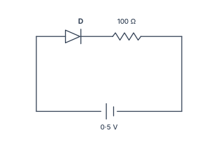
- CBSE 2023Set 55/4/11 markMCQQ.The threshold voltage for a p-n junction diode used in the circuit is 0.7 V. The type of biasing and current in the circuit are : (A) Forward biasing, 0 A (B) Reverse biasing, 0 A (C) Forward biasing, 5 mA (D) Reverse biasing, 2 mA
›Reveal solutionSolution
The diode is forward-biased because the battery’s positive terminal connects to the p-side and negative to the n-side. However, the applied voltage (0.5 V) is less than the threshold voltage (0.7 V), so the diode remains in the “off” state and no current flows. The correct choice is (A).
Figure — CBSE 2023 55/4/1 Q15
The concept: Why a diode doesn’t conduct below its threshold
A p-n junction diode is not a perfect switch that turns on the instant you apply any forward voltage. In forward bias, the external voltage must overcome the built-in potential barrier (about 0.7 V for silicon) before significant current can flow. Below that threshold, the diode’s resistance is extremely high — effectively an open circuit. This is why the circuit current is zero when the battery supplies only 0.5 V.
Watch outA common mistake is to assume that any forward bias automatically produces current. In reality, the diode conducts only when the applied voltage exceeds the threshold (knee) voltage — typically 0.7 V for silicon.
Step-by-step reasoning
-
Identify the biasing from the circuit diagram
The diode symbol shows the p-side (anode) connected to the positive terminal of the 0.5 V cell, and the n-side (cathode) connected to the negative terminal. This is the standard forward-bias configuration: the external field opposes the built-in field, reducing the barrier.
-
Check the applied voltage against the threshold
The battery supplies only 0.5 V. The diode’s threshold voltage is given as 0.7 V. Since 0.5<0.7, the applied voltage is insufficient to overcome the barrier.
-
Determine the diode’s state
In this sub-threshold region, the diode behaves like a very large resistor — practically an open circuit. No charge carriers can cross the junction in significant numbers.
-
Calculate the current
With the diode effectively open, the series circuit is broken. By Ohm’s law, I=RV, but here the diode’s infinite resistance means I=0 A. The 100 Ω resistor plays no role because no current flows through it.
TipYou can think of the diode as a “voltage-controlled switch”: it stays off until the forward voltage reaches the threshold, then turns on abruptly. Below threshold, treat it as an open circuit.
Final answer
✓Final answerThe circuit is forward-biased, but the current is 0 A. The correct option is (A).
-
- CBSE 2023Set ANNUAL1 markQ.Is the Junction diode D forward or reverse biased in the given diagram?

›Reveal solutionSolution
The anode (p-side) of D is connected (through R) to the higher potential (+5 V) terminal and the cathode (n-side) to the lower potential (+2 V) terminal, so D is forward biased.
A junction diode conducts easily (is forward biased) when its p-side (anode) is at a higher potential than its n-side (cathode). Here the anode of D is joined through the resistor R to the +5 V terminal, while the cathode is joined to the +2 V terminal. Since +5 V > +2 V, the anode side is at the higher potential, which drives conventional current from the +5V terminal through R and D to the +2 V terminal — i.e., D is forward biased.
✓Final answerThe junction diode D is forward biased.
🎓Unlock everything free for 14 days
- ✓Full step-by-step solutions
- ✓Concept-first explanations
- ✓Methods, shortcuts & mistakes
- ✓PYQ mapping + timed mock tests
Full access for 14 days. No credit card required.