Physics · Ch 3 — Current Electricity
Limitations of Ohm's Law
Limitations of Ohm's Law
Why Ohm’s Law Has Limits
Ohm’s law states that for many conductors, the current is directly proportional to the applied voltage :
where is a constant resistance. However, this simple proportionality does not hold for all materials and devices. The deviations fall into three main categories.
Type (a): Non‑proportional – relation
For some materials, is not proportional to . The graph of versus is not a straight line through the origin.
- The resistance changes with the applied voltage or current.
- Example: a semiconductor diode at high forward bias.
Type (b): Dependence on the sign of
In certain devices, the current depends on the direction (sign) of the applied voltage.
- If a voltage gives a current , then reversing the voltage to does not produce a current of the same magnitude.
- The – characteristic is asymmetric.
- Example: a diode (studied in Chapter 14) conducts easily in one direction but almost not at all in the reverse direction.
Type (c): Non‑unique – relation
For some materials, the same current can correspond to more than one value of voltage .
- The – curve is multivalued (e.g., an S‑shaped or N‑shaped curve).
- Example: Gallium Arsenide (GaAs) exhibits such behaviour.
Summary of Deviations
| Type | Behaviour | Example |
|---|---|---|
| (a) | not proportional to | Semiconductor diode (forward bias) |
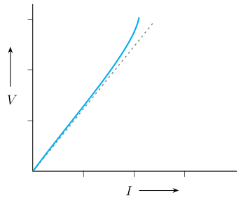
Drawn by us to help you understand the concept clearly, and verified to make sure it's accurate. For exams, practice from your textbook's own diagram.
The graph plots voltage on the vertical axis against current on the horizontal axis, both positive (first quadrant). The origin is at the lower-left corner.
- The solid curve represents the actual behaviour of a good conductor. It starts at the origin, is nearly straight for small , then bends upward (concave-up, super-linear) as increases. This means that at higher currents, the voltage rises faster than a proportional increase — the conductor deviates from Ohm's law.
- The dashed straight line is the ideal Ohm's law prediction: , with constant resistance . It is the tangent to the solid curve near the origin, so at small currents the conductor obeys Ohm's law. At larger currents, the dashed line lies below the solid curve, showing that the actual voltage is greater than the Ohm's law value for the same current.
Physical idea: For a good conductor, Ohm's law holds only up to a certain current. Beyond that, the conductor's resistance increases (often due to heating, which increases lattice vibrations and electron scattering). The graph illustrates limitation (a) from the textbook: "V ceases to be proportional to I."
Key formula developed with this figure is Ohm's law in its ideal form:
where:
- = potential difference across the conductor (volts)
- = current through the conductor (amperes) …
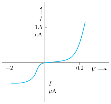
Drawn by us to help you understand the concept clearly, and verified to make sure it's accurate. For exams, practice from your textbook's own diagram.
What the Figure Shows
The figure is a four-quadrant I–V characteristic of a diode, with the axes crossing at the origin. The vertical axis (current ) is scaled differently for positive and negative values: the positive side is labelled in mA (milliamperes), with a marked value of 1.5 mA near the top, while the negative side is labelled in μA (microamperes). The horizontal axis (voltage ) also uses different scales: the positive side extends to about 0.2 V (right), and the negative side goes to –2 V (left). This asymmetry in scales is crucial — it visually emphasises that the diode behaves very differently for forward and reverse voltages.
The Curve and Its Physical Meaning
The curve itself is a stretched-S shape that passes through the origin. In the third quadrant (negative , negative ), the curve runs slightly below the horizontal axis with a shallow dip — this is the reverse bias region, where only a tiny leakage current (on the order of μA) flows. As approaches zero from the negative side, the curve bends gently through the origin (the S-bend). In the first quadrant (positive , positive ), the curve rises sharply after about 0.2 V — this is the forward bias region, where current increases dramatically (to mA levels) once the voltage exceeds a threshold (the forward knee).
This behaviour directly illustrates limitation (b) of Ohm’s law: the relation between and depends on the sign of . Reversing the voltage does not produce a current of the same magnitude in the opposite direction — a diode allows current to flow easily in one direction (forward bias) but blocks it in the other (reverse bias).
Key Formula and Symbol Explanation
The textbook uses this figure to show that Ohm’s law () fails for a diode. Instead, the diode’s current–voltage relation is given by the Shockley diode equation (introduced later in Chapter 14):
Where:
- is the diode current (in amperes, A)
- is the reverse saturation current (a very small constant, typically in μA or nA)
- is the applied voltage (in volts, V)
- is the ideality factor (usually between 1 and 2 for silicon diodes) …
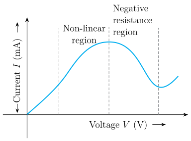
Drawn by us to help you understand the concept clearly, and verified to make sure it's accurate. For exams, practice from your textbook's own diagram.
The graph plots Current (in mA) on the vertical axis against Voltage (in V) on the horizontal axis, both in the first quadrant (positive values only). The curve starts at the origin and rises steeply, but instead of continuing upward linearly, it reaches a rounded peak, then descends into a valley, and finally rises again toward the right. This creates an N-shaped profile: a hump followed by a dip.
Two dashed vertical guide lines partition the curve into distinct regions:
- The ascending part from the origin to the peak is labelled "Non-linear region" — here and are not proportional, but the current still increases with voltage.
- The descending part from the peak down to the valley is labelled "Negative resistance region" — here an increase in voltage causes a decrease in current, which is the opposite of ordinary ohmic behaviour.
The physical idea this figure teaches is that Ohm's law is not universal. Specifically, the graph illustrates type (c) deviation: the relation between and is not unique — for a given current , there can be more than one corresponding voltage . The material shown, GaAs (gallium arsenide), exhibits this N-shaped characteristic, which is exploited in devices like tunnel diodes.
The key formula the textbook develops with this figure is the definition of resistance in the context of non-ohmic materials. For any device, the static resistance (or DC resistance) at a point is given by:
where is the voltage across the device and is the current through it. However, in the negative resistance region, the dynamic resistance (or differential resistance) is negative:
…