Chemistry · Ch 16 — Green Chemistry and Nanochemistry
Photographs of Instruments
Photographs of Instruments
This section presents photographs and labelled schematic diagrams of the actual instruments named in Table 16.1 (Section 16.7.3), giving the reader a visual sense of what the analytical equipment used to characterise nanomaterials actually looks like in practice, alongside a timeline figure of key contributors to the development of nanotechnology as a field. The instruments shown are the X-ray diffractometer (Fig 16.8), the scanning electron microscope (a schematic diagram in Fig 16.9 and a photograph in Fig 16.10), the transmission electron microscope (a fully labelled schematic diagram, Fig 16.11), and the FTIR spectrophotometer (Fig 16.12). Fig 16.13 supplements these instrument photographs with a timeline of scientists and organisations that contributed to nanotechnology's development, spanning Watson and Crick's 1953 DNA structur …
What this figure shows. A photograph of a bench-top X-ray diffractometer, the instrument used for X-ray diffraction (XRD) analysis (Table 16.1), which determines a nanomaterial's particle size, crystal structure and geometry by measuring how X-rays are diffracted by the sample's crystal l …
Drawn by us to help you understand the concept clearly, and verified to make sure it's accurate. For exams, practice from your textbook's own diagram.
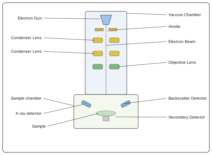
What this figure shows. A labelled schematic cross-section of a scanning electron microscope (SEM), showing its main internal components in sequence from top to bottom: the electron gun and its anode generating the electron beam, condenser lenses (shown twice) that focus and narrow the beam, the objective lens that further focuses the beam onto the sample, the vacuum chamber housing the whole optical column, the sample chamber holding the specimen being imaged, and, around the sample, the backscatter detector, secondary detector and X-ray detector that together collect the different signals generated when the electron beam strikes the sample surface -- these signals are what SEM uses to …
What this figure shows. A photograph of a complete, real scanning electron microscope (SEM) instrument, showing the physical form of the equipment whose internal optical layout is diagrammed separately in Fig 16.9. Placing the labelled schematic (Fig 16.9) and this photograph side by side lets the reader match each internal component named in the schematic -- the electron gun, condenser and objective lenses, sample chamber and detectors -- to its actual position on the real bench-top instrument used to determine surfa …
Drawn by us to help you understand the concept clearly, and verified to make sure it's accurate. For exams, practice from your textbook's own diagram.
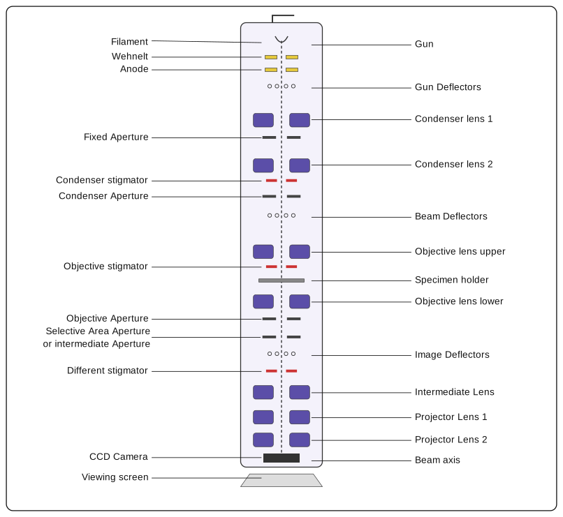
What this figure shows. A detailed labelled schematic cross-section of a transmission electron microscope (TEM), showing, from top to bottom, the electron gun, filament and Wehnelt cylinder generating the beam, the anode and fixed/condenser apertures, two condenser lenses with their own stigmators and beam deflectors that shape and focus the beam, the specimen holder where the sample sits, upper and lower objective lenses (with their own aperture, stigmator and image deflectors) that focus the beam that has passed through the thin specimen, an intermediate lens, a selective-area/intermediate aperture, two projector lenses, and finally the imaging system -- a viewing screen and a CCD camera -- at the bottom of the column, along with the overall beam axis running down the centre of the instrument. TEM's transmitted-beam design is what gives it its characteristic strength: measuring particle size (Table 16.1) by ima …
What this figure shows. A photograph of an FTIR (Fourier transform infrared) spectrophotometer, the instrument used for FTIR spectroscopy (Table 16.1), which identifies the functional groups present in a nanomaterial sample and gives information about its chemical binding nature by measuring the infrared radiation the samp …
Drawn by us to help you understand the concept clearly, and verified to make sure it's accurate. For exams, practice from your textbook's own diagram.
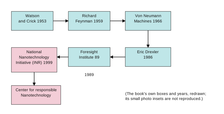
What this figure shows. A timeline figure listing key milestones and contributors in the development of nanotechnology as a field, in roughly chronological order: Watson and Crick, 1953 (the discovery of the double-helix structure of DNA, an early landmark in understanding molecular-scale structure); Richard Feynman, 1959 (whose talk 'There's Plenty of Room at the Bottom' is widely credited as an early conceptual foundation for nanotechnology); Von Neumann machines, 1966 (the concept of self-replicating machines); Eric Drexler, 1986 (whose writing helped popularise molecular nanotechnology as a field); the Foresight Institute, founded 1986/89 (a nanotechnology advocacy and research organisation); the Center for Responsible Nanotechnology; and the (US) National Nanotechnology Initiative, 1999/2000 -- together illustrating that nanotechnology's development drew on contributions spanning molecular biology, theoretical physics, computing theor …