Chemistry · Ch 1 — Solid State
Extrinsic semiconductors and doping
Extrinsic semiconductors and doping
The conductivity of a semiconductor can be increased deliberately by doping -- adding a minute, controlled quantity of an impurity, called the dopant, to the pure material. A doped semiconductor, having higher conductivity than the pure (intrinsic) semiconductor, is called an extrinsic semiconductor. There are two types.
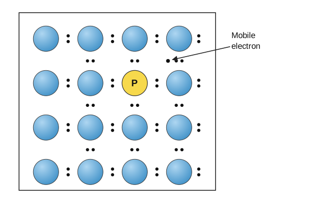
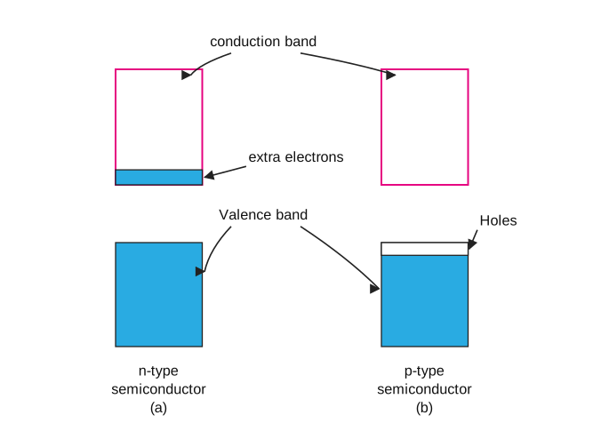
i. n-type semiconductor : An n-type semiconductor is obtained by doping a group-14 semiconductor (Si or Ge) with a group-15 element such as P, As, Sb or Bi. Consider silicon doped with phosphorus: the P atoms occupy some of the regular lattice sites of the Si atoms, without disturbing the crystal structure (Fig. 1.26). Phosphorus has five valence electrons, and only four of them are needed to bond with the four neighbouring Si atoms -- the fifth electron is left over, and it enters the conduction band (Fig. 1.27a). An n-type semiconductor therefore carries extra electrons in its conduction band ('n' for the negative charge carriers), and its conductivity is higher than that of pure silicon.
Drawn by us to help you understand the concept clearly, and verified to make sure it's accurate. For exams, practice from your textbook's own diagram.
What this figure shows. A 4-by-4 grid of shaded silicon atoms whose bonds are drawn as pairs of dots (shared electron pairs) between neighbours. One regular site in the second row is occupied instead by a yellow circle labelled . Because phosphorus brings five valence electrons and only four are used in bonds, one extra electron is drawn as a free dot beside the P atom, pointed out by a straight arrow labelled …
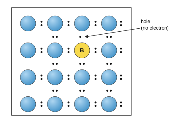
ii. p-type semiconductor : A p-type semiconductor is obtained by doping Si or Ge with a group-13 element such as B, Ga or In. Boron has only three valence electrons, so a B atom occupying a regular Si lattice site (Fig. 1.28) can bond with only three of its four Si neighbours -- the fourth bonding position is an electron vacancy, called a hole. A hole behaves as though it carries a positive charge ('p' for positive): under an applied potential, a neighbouring valence electron hops into the hole and leaves a new hole behind, so the holes effectively travel through the valence band (Fig. 1.27b) in the direction opposite to that of the electrons.
Drawn by us to help you understand the concept clearly, and verified to make sure it's accurate. For exams, practice from your textbook's own diagram.
What this figure shows. The same 4-by-4 dot-bonded silicon grid as Fig. 1.26, but the substituted atom in the second row is a yellow circle labelled . Boron brings only three valence electrons, so one bonding position next to the B atom is missing a dot -- an electron vacancy pointed out by a straight arrow labelled 'hole (no electr …
Drawn by us to help you understand the concept clearly, and verified to make sure it's accurate. For exams, practice from your textbook's own diagram.
What this figure shows. Two paired band diagrams. Panel (a), 'n-type semiconductor': an empty conduction band carrying a thin filled strip along its bottom edge -- pointer arrows label the 'conduction band', the thin strip as 'extra electrons', and the solid lower bar as 'Valence band'. Panel (b), 'p-type semiconductor': an empty conduction band above a filled valence band whose top edge carries a thin EMPTY strip, labelled 'Holes' by a pointer arrow. The extra conduction-band electrons of n-type and the valence-band holes of p-type a …
…