Q.Answer the following, giving reason :
You're viewing a preview — the full solution, concept, methods & PYQ mapping are locked.
Start your 14-day free trial to unlock the full solution →A p-n junction’s resistance depends on bias because forward bias narrows the depletion layer (allowing large current), while reverse bias widens it (blocking current). Doping introduces mobile charge carriers, making semiconductors conductive enough for devices. Photodiodes use reverse bias to create a wide depletion region that efficiently separates photo-generated electron-hole pairs, producing a measurable photocurrent.
(a) Why p-n junction resistance is low in forward bias and high in reverse bias
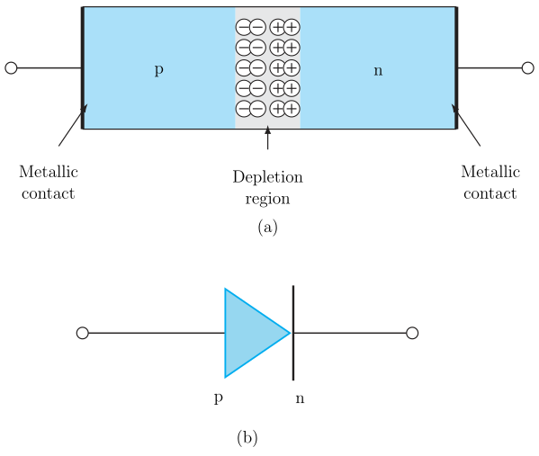
The key lies in the depletion layer — the region near the junction that is depleted of free charge carriers. This layer acts like a barrier.
-
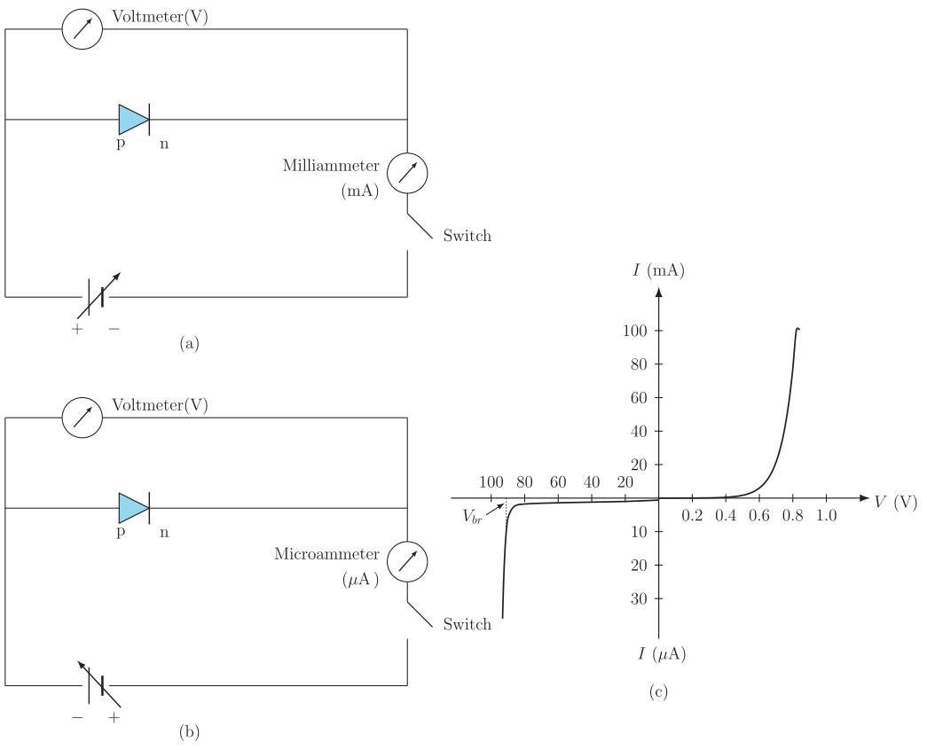
Forward bias: The positive terminal of the battery is connected to the p-side, negative to the n-side. This reduces the built-in potential barrier. The depletion layer narrows. Majority carriers (holes from p-side, electrons from n-side) can now easily cross the junction. A small increase in voltage produces a large current — the junction offers low resistance.
-
Reverse bias: The positive terminal is connected to the n-side, negative to the p-side. This increases the barrier height. The depletion layer widens. Majority carriers are pulled away from the junction, so almost no current flows. Only a tiny leakage current (due to minority carriers) exists. The junction therefore shows very high resistance.
A common mistake is to think resistance is constant. In forward bias, resistance is dynamic — it decreases sharply as voltage increases beyond the knee voltage (≈0.7 V for Si). In reverse bias, resistance is extremely high (megaohms) until breakdown.
Dynamic resistance: — in forward bias, is small (tens of ohms); in reverse bias, is very large (MΩ).
(b) Why doping is necessary for making electronic devices
Intrinsic (pure) semiconductors like silicon or germanium have very few free charge carriers at room temperature — about for Si. This gives them high resistivity (≈ for Si), making them behave almost like insulators.
-
Doping introduces impurity atoms (pentavalent for n-type, trivalent for p-type) that donate or accept electrons. This dramatically increases the number of charge carriers — by factors of to .
-
For a p-n junction diode, we need two distinct regions — one with excess electrons (n-type) and one with excess holes (p-type). Without doping, you cannot create this asymmetry. The junction itself is the heart of almost every semiconductor device: diodes, transistors, solar cells, LEDs.
-
Doping also allows us to control conductivity precisely. By choosing the doping concentration, we can tailor the device’s breakdown voltage, switching speed, and current capacity.
Think of doping as adding a pinch of salt to water — pure water barely conducts, but salt water conducts easily. Similarly, a tiny amount of dopant (1 part in ) can increase conductivity by a factor of .
(c) Why photodiodes are operated in reverse bias …
Unlock everything free for 14 days
- Full step-by-step solutions
- Concept-first explanations
- Methods, shortcuts & mistakes
- PYQ mapping + timed mock tests
Full access for 14 days. No credit card required.