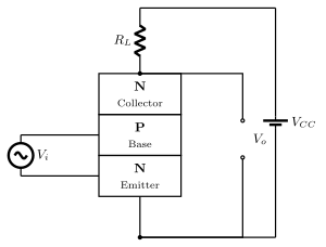
Q.Draw a Circuit diagram for studying V-I characteristics for a transistor in common emitter (CE) configuration. Draw and explain its typical output V-I characteristics. OR Explain the working of common emitter transistor amplifier using circuit diagram.
You're viewing a preview — the full solution, concept, methods & PYQ mapping are locked.
Start your 14-day free trial to unlock the full solution →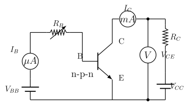
The CE output-characteristic circuit varies V_CE at a fixed I_B and plots the resulting I_C; repeating for several I_B values gives a family of curves showing the transistor's active, saturation and cutoff regions.
Circuit: an NPN transistor is used with the emitter common to both input and output loops. The input loop has a battery (through a variable resistor / microammeter) forward-biasing the base–emitter junction, setting a base current . The output loop has a battery (through a variable resistor / milliammeter) reverse-biasing the collector–base junction, providing collector–emitter voltage and collector current .
Procedure: for a fixed value of (set via the input loop), is varied over a range and the corresponding is measured and plotted. This is repeated for several different fixed values of , giving a family of output curves ( vs , one curve per ).
…
Unlock everything free for 14 days
- Full step-by-step solutions
- Concept-first explanations
- Methods, shortcuts & mistakes
- PYQ mapping + timed mock tests
Full access for 14 days. No credit card required.