Q.Draw a circuit diagram to study the input and output characteristics of an n-p-n transistor in common-emitter configuration. Draw the typical input and output characteristics. (1+1+1) OR What is logic symbol and truth table for NAND gate? How is it used to obtain OR gate? (1+1+1)
You're viewing a preview — the full solution, concept, methods & PYQ mapping are locked.
Start your 14-day free trial to unlock the full solution →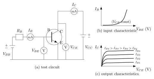
The circuit biases both junctions independently through separate supplies, letting you record how base current controls the emitter-base voltage (input) and how collector current depends on collector-emitter voltage for each base current (output).
Circuit (described): An n-p-n transistor is connected in common-emitter (CE) configuration: the emitter is common to both the input and output loops (grounded). The base-emitter junction is connected to a variable voltage supply (through a base resistor and a milliammeter to measure , with a voltmeter across base-emitter to read ) forming the input circuit. The collector-emitter junction is connected to a variable voltage supply (through a milliammeter to measure , with a voltmeter across collector-emitter to read ) forming the output circuit.
Input characteristics: obtained by plotting base current (y-axis) against base-emitter voltage (x-axis), keeping the collector-emitter voltage constant. The curve resembles that of a forward-biased diode: stays negligible until crosses a threshold (~0.7 V for silicon), after which it rises steeply.
…
Unlock everything free for 14 days
- Full step-by-step solutions
- Concept-first explanations
- Methods, shortcuts & mistakes
- PYQ mapping + timed mock tests
Full access for 14 days. No credit card required.