Question 87 of 88
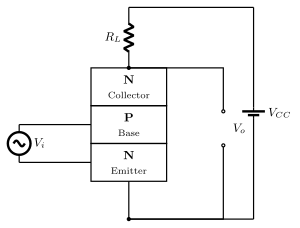
Q.Draw the schematic circuit diagram for a NPN transistor in common emitter configuration.
Tamil Nadu DgeTamil Nadu HSC (DGE) Board 2026Subjective· 2mImportance★★★★★
99% · 87/88 Questions
You're viewing a preview — the full solution, concept, methods & PYQ mapping are locked.
Start your 14-day free trial to unlock the full solution →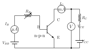
In an NPN common-emitter circuit, the emitter is the common terminal; the base-emitter junction (forward biased) forms the input loop, and the collector (through a load resistor to the supply) forms the output loop, with the emitter grounded.
Circuit description
In the common-emitter (CE) configuration:
              +Vcc
               |
              R_C
               |
input --[Cin]--o---- Base    Collector ----o--[Cout]-- output
     (with bias           NPN            (across R_C)
      resistors R1,R2)   transistor
                          Emitter
                             |
                           ground (common to input and output)
- The emitter is grounded/common to both the input and output loops (hence "common emitter").
- Input circuit: base-emitter junction, forward biased by a voltage-divider (or base-resistor) network, with the small AC signal coupled in via a capacitor at the base. …
Unlock everything free for 14 days
- Full step-by-step solutions
- Concept-first explanations
- Methods, shortcuts & mistakes
- PYQ mapping + timed mock tests
Full access for 14 days. No credit card required.