Question 73 of 88
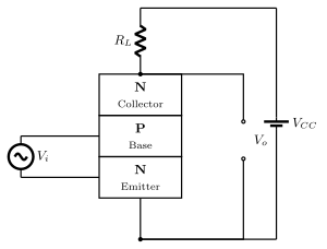
Q.Draw the circuit diagram of NPN transistor in Common Emitter Configuration.
Tamil Nadu DgeTamil Nadu HSC (DGE) Board 2022Subjective· 3mImportance★★★★★
83% · 73/88 Questions
You're viewing a preview — the full solution, concept, methods & PYQ mapping are locked.
Start your 14-day free trial to unlock the full solution →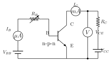
In an NPN transistor's CE circuit, the emitter is the common (grounded) terminal shared by input and output loops, the base is biased through an input resistor from the signal source, and the collector draws current through a load resistor from the supply.
Circuit description (common-emitter configuration, NPN transistor)
- Emitter (E): connected to the common/ground line, shared by both the input loop and the output loop — this is why the configuration is called 'common emitter'.
- Base (B): connected through a base resistor to the input voltage source (biased so the base-emitter junction is forward biased); the input signal is applied here, across the base-emitter junction.
- Collector (C): connected through a load (collector) resistor to the DC supply (so the collector-base junction is reverse biased); the output is taken across the collector and the emitter (i.e. across the transistor and combination).
- The arrow on the emitter (pointing outward, away from the base, for an NPN transistor) indicates the conventional current direction out of the emitter terminal. …
Unlock everything free for 14 days
- Full step-by-step solutions
- Concept-first explanations
- Methods, shortcuts & mistakes
- PYQ mapping + timed mock tests
Full access for 14 days. No credit card required.