Electronics · Ch 10 — Digital Electronics
Logic gates
Logic gates
A logic gate is an electronic circuit that operates on the rules of Boolean algebra to carry out one particular logic function; gates are the basic elements from which every digital system is assembled. Each gate accepts one or more binary inputs and produces a single binary output that depends only on the present combination of inputs, which is captured in its truth table.
The textbook lists seven types of gate: the three basic gates AND, OR, NOT; the two universal gates NAND and NOR; and the two combinational gates exclusive-OR (XOR) and exclusive-NOR (XNOR). This section studies XOR, XNOR, NAND and NOR in detail — their symbols, Boolean expressions, truth tables, IC pin diagrams, timing diagrams and gate realizations.
Exclusive-OR (XOR) gate
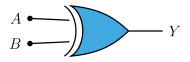
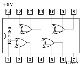
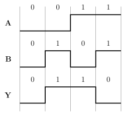
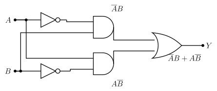
The XOR gate gives a HIGH output only when an odd number of its inputs are HIGH. For two inputs this means the output is 1 whenever the inputs are different, which is why it is also called an inequality detector. Its Boolean expression is , read as "Y equals A XOR B". XOR gates are available as ICs — IC 7486 contains four independent 2-input XOR gates (figure 10.1.2). XOR gates are widely used in magnitude comparators, gray-code converters, adders and subtractors, odd-parity checkers and modulo-2 adders. The XOR waveform behaviour is shown in the timing diagram (figure 10.1.3), and figure 10.1.4 shows how an XOR is realized from two NOT, two AND and one OR gate.
Exclusive-NOR (XNOR) gate
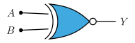
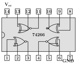
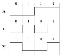
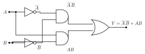
The XNOR gate is the complement of the XOR gate: its output is HIGH only when both inputs are the same, so it is also called a coincidence gate. It behaves like an XOR gate followed by an inverter. Its expression is . IC 74266 contains four 2-input XNOR gates (figure 10.1.6). The XNOR gate is used in comparators and even-parity checkers. Its timing diagram is figure 10.1.7, and figure 10.1.8 shows its realization using two NOT, two AND and one OR gate.
NAND gate — a universal gate
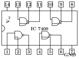
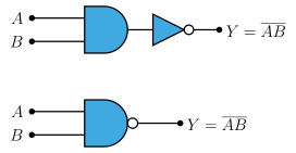
The NAND gate (NOT-AND) gives a LOW output only when all inputs are HIGH; equivalently, its output is HIGH when any one input is LOW. Its expression is . IC 7400 is a quad 2-input NAND (figure 10.1.9), and figure 10.1.10 shows the symbol (an AND shape with an output bubble, equivalent to an AND gate followed by an inverter).
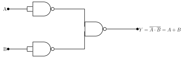
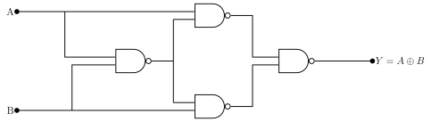
NAND is called a universal gate because every other gate can be built from NAND gates alone: the NOT function by tying both inputs together (figure 10.1.12, ); the AND function using two NANDs (figure 10.1.13, ); the OR function using three NANDs (figure 10.1.14); and even the XOR function using four NANDs (figure 10.1.15).
The official KTBS corrigendum corrects the printed label of figure 10.1.14 (OR using NAND) from to . The correct working is that feeding and into a NAND gives by De Morgan's theorem — an OR gate.
NOR gate — a universal gate …
An electronic circuit that works on the rules of Boolean algebra to perform one particular logic function. Logic gates are the basic elements of every digital system; each has one or more binary inputs and a single binary output. The seven types are the basic gates (AND, OR, NOT), the universal gate …
Drawn by us to help you understand the concept clearly, and verified to make sure it's accurate. For exams, practice from your textbook's own diagram.
The standard XOR symbol (figure 10.1.1): an OR-gate curved shape with an extra curved line across the two inputs A (top) and B (bottom); the single output Y carries no inversion bubble. Read with its truth table, only when A and B differ, …
— output HIGH only when the two inputs differ (an odd number of HIGH inputs). Here is the XOR operator and the overbar is complement; the term covers A=0,B=1 and covers A=1,B=0. U …
| A | B | Y = A ⊕ B |
|---|---|---|
| 0 | 0 | 0 |
| 0 | 1 | 1 |
Drawn by us to help you understand the concept clearly, and verified to make sure it's accurate. For exams, practice from your textbook's own diagram.
Figure 10.1.2: 14-pin DIP labelled IC 7486 with a notch on the left. Pin 14 = +5V, pin 7 = GND. The four XOR gates are wired inputs 1,2 → output 3; inputs 4,5 → output 6; inputs 9,10 → ou …
Drawn by us to help you understand the concept clearly, and verified to make sure it's accurate. For exams, practice from your textbook's own diagram.
Figure 10.1.3: three stacked waveforms A, B, Y. A = 0,0,1,1; B = 0,1,0,1; Y = 0,1,1,0 — matching the XOR truth table. Reading the pattern: Y follows A XOR B in each column — HIGH only where A and B differ (columns 2 and 3), LOW where they match (columns 1 a …
Drawn by us to help you understand the concept clearly, and verified to make sure it's accurate. For exams, practice from your textbook's own diagram.
Figure 10.1.4: A and B each feed an inverter to give and ; an upper AND forms , a lower AND forms ; a final OR gives $Y …
Drawn by us to help you understand the concept clearly, and verified to make sure it's accurate. For exams, practice from your textbook's own diagram.
Figure 10.1.5: the XOR shape with a small inversion bubble on the output; inputs A (top) and B (bottom), output Y. The output bubble marks inversion of the XOR result, so this XNOR gives only when A and B are equal (a coincidence gate) — …
— output HIGH only when both inputs are the same (a coincidence gate). The overbar on inverts the XOR, so only when the inputs match: covers 0,0 and covers …
| A | B | Y = ̅(A ⊕ B) |
|---|---|---|
| 0 | 0 | 1 |
| 0 | 1 | 0 |
Drawn by us to help you understand the concept clearly, and verified to make sure it's accurate. For exams, practice from your textbook's own diagram.
Figure 10.1.6: 14-pin DIP labelled 74266 with a left notch. Pin 14 = Vcc, pin 7 = GND; four 2-input XNOR gates drawn inside. What to notice: like every quad DIP it packs four independent 2-input gates powered from the single /GND pair, so one IC supplies four X …
Drawn by us to help you understand the concept clearly, and verified to make sure it's accurate. For exams, practice from your textbook's own diagram.
Figure 10.1.7: waveforms A = 0,0,1,1; B = 0,1,0,1; Y = 1,0,0,1 — matching the XNOR truth table. Reading the pattern: Y is HIGH wherever A and B agree (columns 1 and 4: 0,0 and 1,1) and LOW wherever they differ (columns 2 and 3), the exact complement of the XOR wave …
Drawn by us to help you understand the concept clearly, and verified to make sure it's accurate. For exams, practice from your textbook's own diagram.
Figure 10.1.8: A and B each feed an inverter; an upper AND forms , a lower AND forms ; a final OR gives . Notice this is the XOR realization with the two AND terms swapped: it collects the matching cases and …
A NOT-AND gate whose output is LOW only when all inputs are HIGH, i.e. HIGH when any one input is LOW; . It is called a universal gate because NOT, AND, OR and XOR can all be built from NAND gates …
Drawn by us to help you understand the concept clearly, and verified to make sure it's accurate. For exams, practice from your textbook's own diagram.
Figure 10.1.9: 14-pin DIP labelled IC 7400, pin 14 = Vcc, pin 7 = GND; NAND gates wired inputs 1,2 → 3; 4,5 → 6; 9,10 → 8; 12,13 → 11. What to notice: the four NAND gates share one /GND pair; because NAND is a universal gate, this single IC can be wired to …
Drawn by us to help you understand the concept clearly, and verified to make sure it's accurate. For exams, practice from your textbook's own diagram.
Figure 10.1.10: (top) an AND gate followed by an inverter; (bottom) a single AND shape with an output bubble. Inputs A, B, output . The bubble on the output is the key detail: it inverts the AND result, giving — LOW only when both inputs are HIGH, HIGH otherwise.
[!NOTE] The textbook's printed label for this figure (and the matching truth-table header) writes the NAND output with two separate bars, , which reads as — that contradicts the book's own NAND truth table (output 1,1,1,0). The correct NAND output, used here and consistent with that truth table, is …
— output HIGH when any input is LOW; LOW only when all inputs are HIGH. The overbar covers the whole product , so the AND is formed first and then inverted. The output is LOW only for A=B=1 and HIGH for every other combination; NAND is a univer …
| A | B | Y = ̅(AB) |
|---|---|---|
| 0 | 0 | 1 |
| 0 | 1 | 1 |
Drawn by us to help you understand the concept clearly, and verified to make sure it's accurate. For exams, practice from your textbook's own diagram.
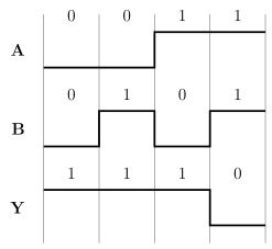
Figure 10.1.11: waveforms A = 0,0,1,1; B = 0,1,0,1; Y = 1,1,1,0 — matching the NAND truth table. Reading the pattern: Y stays HIGH for the first three columns (where at least one input is LOW) and drops LOW only in the last column, where both A and B are H …

Drawn by us to help you understand the concept clearly, and verified to make sure it's accurate. For exams, practice from your textbook's own diagram.
Figure 10.1.12: a 2-input NAND with both inputs tied to a common input A gives — an inverter. What to notice: tying both NAND inputs to A makes the product , and the NAND then inverts it, so a universal NAN …

Drawn by us to help you understand the concept clearly, and verified to make sure it's accurate. For exams, practice from your textbook's own diagram.
Figure 10.1.13: a NAND of A and B followed by a NAND wired as an inverter gives . What to notice: the first NAND gives and the second, wired as an inverter, cancels the bar to recover the true AND — two u …
Drawn by us to help you understand the concept clearly, and verified to make sure it's accurate. For exams, practice from your textbook's own diagram.
Figure 10.1.14: A and B each pass through a NAND-inverter to give and ; these feed a third NAND giving by De Morgan's theorem. (The printed figure label is corrected per the official …
Drawn by us to help you understand the concept clearly, and verified to make sure it's accurate. For exams, practice from your textbook's own diagram.
Figure 10.1.15: a central NAND of A and B feeds two intermediate NANDs (with A and with B), whose outputs feed a final NAND giving . What to notice: four universal NAND gates alone reproduce the XOR function , HIGH only when A and B differ — proof …
A NOT-OR gate whose output is HIGH only when all inputs are LOW; the complement of the OR gate, . It is a universal gate because NOT, OR, AND and XNOR can all be built from NOR gates …

Drawn by us to help you understand the concept clearly, and verified to make sure it's accurate. For exams, practice from your textbook's own diagram.
Figure 10.1.16: an OR-gate curved shape with a small inversion bubble on the output; inputs A, B, output . The bubble on the output inverts the OR result, giving — HIGH only when both A and B are LOW; …
— output HIGH only when all inputs are LOW. The overbar covers the whole sum , so the OR is taken first and then inverted. The output is HIGH only when every input is LOW and LOW if any input is HIGH; NOR is a universal gate fro …
| A | B | Y = ̅(A+B) |
|---|---|---|
| 0 | 0 | 1 |
| 0 | 1 | 0 |
Drawn by us to help you understand the concept clearly, and verified to make sure it's accurate. For exams, practice from your textbook's own diagram.
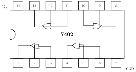
Figure 10.1.17: 14-pin DIP labelled 7402, pin 14 = Vcc, pin 7 = GND; four 2-input NOR gates drawn inside. What to notice: the four NOR gates share the single /GND pair, and because NOR is a universal gate this one IC can be wired to reali …
Drawn by us to help you understand the concept clearly, and verified to make sure it's accurate. For exams, practice from your textbook's own diagram.
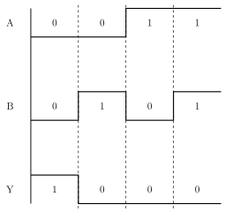
Figure 10.1.18: waveforms A = 0,0,1,1; B = 0,1,0,1; Y = 1,0,0,0 — matching the NOR truth table. Reading the pattern: Y is HIGH only in the first column, where both A and B are LOW, and stays LOW for the other three columns where at least one input is H …

Drawn by us to help you understand the concept clearly, and verified to make sure it's accurate. For exams, practice from your textbook's own diagram.
Figure 10.1.19: a 2-input NOR with both inputs tied to a common input A gives . What to notice: tying both NOR inputs to A makes the sum , which the NOR then inverts, so a single uni …

Drawn by us to help you understand the concept clearly, and verified to make sure it's accurate. For exams, practice from your textbook's own diagram.
Figure 10.1.20: a NOR of A and B followed by a NOR wired as an inverter gives . What to notice: the first NOR gives and the second, wired as an inverter, removes the bar to recover the true OR — tw …
Drawn by us to help you understand the concept clearly, and verified to make sure it's accurate. For exams, practice from your textbook's own diagram.
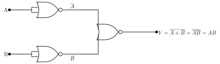
Figure 10.1.21: A and B each pass through a NOR-inverter to give and ; these feed a third NOR giving $Y = \overline{\overline{A} + \overline{B} …
Drawn by us to help you understand the concept clearly, and verified to make sure it's accurate. For exams, practice from your textbook's own diagram.
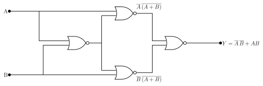
Figure 10.1.22: a first NOR of A and B feeds two intermediate NORs (with A and with B), whose outputs feed a final NOR giving . What to notice: four universal NOR gates alone reproduce the XNOR function, HIGH only when A and B are equal — …