Electronics · Ch 10 — Digital Electronics
Registers
Registers
A register is a group of flip-flops used together to store binary data. Its storage capacity is simply the number of bits (0s and 1s) it can hold, so an -flip-flop register stores bits. Loading a register means setting or resetting its individual flip-flops so that they together hold the desired pattern of bits.
Types of registers
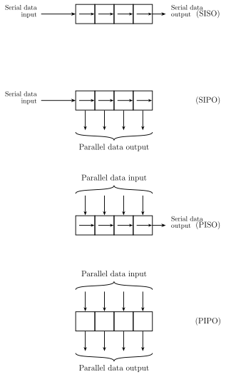
Data can enter a register serially (one bit per clock pulse) or in parallel (all bits at once), and it can leave the register serially (one bit at a time) or in parallel (the whole word available simultaneously). Combining the input and output styles gives four operating modes (Figure 10.6.1):
- Serial-in, Serial-out (SISO)
- Serial-in, Parallel-out (SIPO)
- Parallel-in, Serial-out (PISO)
- Parallel-in, Parallel-out (PIPO)
A register that takes its data in serially is called a shift register. Level-triggered flip-flops are avoided in registers because they create timing problems; edge-triggered or master-slave flip-flops are used instead.
(a) Serial-in, Serial-out (SISO) shift register
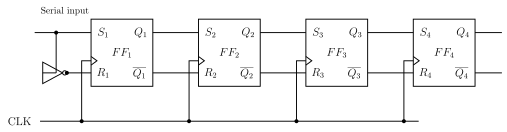
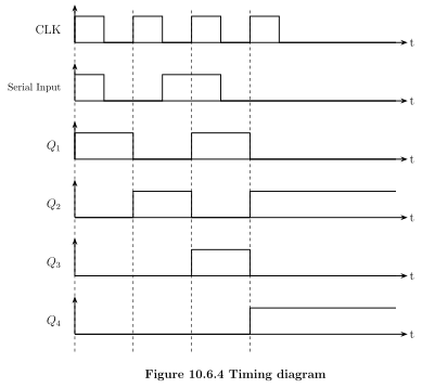
A SISO register can be built from SR or JK flip-flops. A four-bit SISO register using SR flip-flops (Figure 10.6.2) stores up to 4 bits: the serial data enters the S input of the first flip-flop (its complement is fed to R through an inverter), drives the S input of the second, the third, and so on, with the final output taken at . On each positive clock edge every stored bit shifts one stage to the right and a new bit enters the first stage; the bit in the last stage shifts out. As an example, starting from a fully reset register (all 0s) and feeding in the data 0101 serially, the loading is tabulated in Table 10.6.3 and drawn in Figure 10.6.4. Reading the stored 0101 back out serially again takes four clock pulses (Table 10.6.5).
(b) Serial-in, Parallel-out (SIPO) shift register
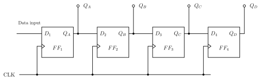
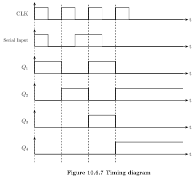
A four-bit SIPO register using D flip-flops (Figure 10.6.6) accepts its data serially, one bit per clock, but once all bits are stored each bit is available at once on its own output line rather than emerging one at a time — the outputs are read in parallel (timing in Figure 10.6.7).
(c) Parallel-in, Serial-out (PISO) shift register
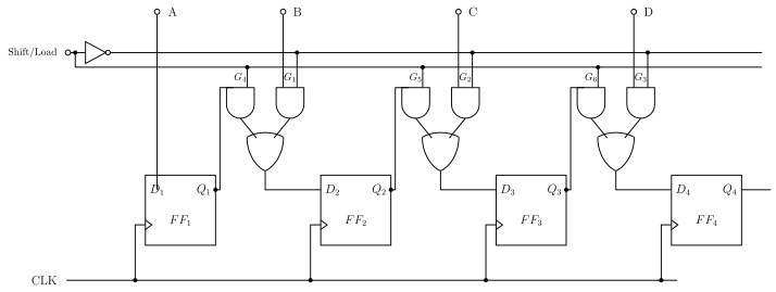
A PISO register loads all its bits simultaneously but transfers them out serially, bit by bit over a single line. In the four-bit PISO register using D flip-flops (Figure 10.6.8), four data lines A, B, C and D allow parallel entry, and a SHIFT/LOAD control (whose LOAD action is active-LOW) selects the mode. When the SHIFT/LOAD line is LOW, gates G4, G5, G6 are disabled and G1, G2, G3 are enabled, so the parallel data appear at the D inputs and one clock pulse loads them to the outputs. When the line is HIGH, G1, G2, G3 are disabled and G4, G5, G6 are enabled, so the stored bits shift right one stage at a time and leave serially at . An OR gate at each stage lets the same flip-flop accept either the shifted bit or the parallel-loaded bit, depending on the control level.
(d) Parallel-in, Parallel-out (PIPO) shift register …
A register is a set of flip-flops used to store binary data. Its storage capacity equals the number of bits it can retain, and loading a register means setting or resetting its flip-flops …
A shift register is a register that accepts its data serially, shifting the stored bits one stage along on each clock pulse. Its four modes — SISO, SIPO, PISO and PIPO — differ in whether data enters …
Drawn by us to help you understand the concept clearly, and verified to make sure it's accurate. For exams, practice from your textbook's own diagram.
Figure 10.6.1 shows the four ways data moves through a register: serial-in/serial-out (SISO), serial-in/parallel-out (SIPO), parallel-in/serial-out (PISO) and parallel-in/parallel-out (PIPO), each drawn as a four-box chain with the appropriate …
Drawn by us to help you understand the concept clearly, and verified to make sure it's accurate. For exams, practice from your textbook's own diagram.
Figure 10.6.2 shows a four-bit serial-in serial-out register using SR flip-flops: the serial input enters (its complement reaching via an inverter), each output drives the next stage's S input, a common clock feeds all four flip-flo …
Pulse 0 is the initial (fully reset) state; the data 0101 is fed in one bit per clock pulse.
| After clock pulse | Serial input | ||||
|---|---|---|---|---|---|
| 0 | 1 | 0 | 0 | 0 | 0 |
| 1 | 0 | 1 | 0 | 0 | 0 |
| 2 | 1 | 0 | 1 | 0 | 0 |
Drawn by us to help you understand the concept clearly, and verified to make sure it's accurate. For exams, practice from your textbook's own diagram.
Figure 10.6.4 plots CLK, the serial input and –, showing the bits of 0101 being clocked in one stage at a time as each flip-flop passes its stored bit to the next. Reading the pattern: on each clock a new bit enters and every stored bit moves one stage to the right, so after f …
The stored word leaves LSB-first at ; a further serial 0 is fed in to reset each stage. Pulse 4 is the final (all-zero) state.
| After clock pulse | Serial input (to reset the flip-flop) | ||||
|---|---|---|---|---|---|
| 0 | 0 | 0 | 1 | 0 | 1 |
| 1 | 0 | 0 | 0 | 1 | 0 |
Drawn by us to help you understand the concept clearly, and verified to make sure it's accurate. For exams, practice from your textbook's own diagram.
Figure 10.6.6 shows a four-bit SIPO register of D flip-flops: data enters serially at , each drives the next D input, and all four outputs – are read together in …
Drawn by us to help you understand the concept clearly, and verified to make sure it's accurate. For exams, practice from your textbook's own diagram.
Figure 10.6.7 plots the clock, serial input and the four outputs, showing the serially entered bits appearing on the parallel output lines. Reading the pattern: bits enter one per clock at the serial input, and once all four are stored they appear together on –$Q_D …
Drawn by us to help you understand the concept clearly, and verified to make sure it's accurate. For exams, practice from your textbook's own diagram.
Figure 10.6.8 shows a four-bit PISO register: four data lines A, B, C, D allow parallel loading, and the SHIFT/LOAD control (LOAD active-LOW) selects — through gate pairs G1–G3 and G4–G6 and an OR gate per stage — whether the register loads in parallel or …
Drawn by us to help you understand the concept clearly, and verified to make sure it's accurate. For exams, practice from your textbook's own diagram.
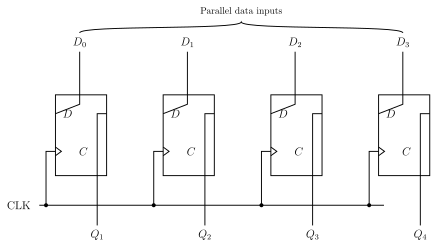
Figure 10.6.11 shows a four-bit PIPO register: the parallel inputs – are applied to the D terminals of the flip-flops and, on the positive clock edge, transferred together to the outputs –. (The book's figure numbering jumps from 10.6.8 …