Electronics · Ch 10 — Digital Electronics
Sequential Logic Circuits
Sequential Logic Circuits
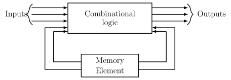
Logic circuits fall into two broad families. Combinational logic circuits produce an output that depends only on the input levels present at that same instant, so they keep no record of what came before — they have no memory. Sequential logic circuits produce outputs that depend on the present inputs and on the sequence of past inputs, so they must store information — they have memory. A sequential circuit is therefore built from a combinational block together with one or more memory elements, whose stored state is fed back into the combinational logic (Figure 10.5.1). The flip-flops, registers and counters covered here make sequential logic one of the highest-yield topics in the Karnataka 2nd PUC Electronics course, and questions on them appear routinely in the II PUC board exam.
The clock and why it matters
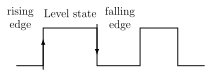
The memory elements in a sequential circuit are meant to change only at fixed, discrete instants rather than continuously. A clock — a device that produces a periodic train of pulses — provides this timekeeping so that every element updates in step. An ideal system clock is a perfectly periodic square wave (Figure 10.5.2(a)). A single clock pulse has three features (Figure 10.5.2(b)): a rising (leading) edge where it goes LOW→HIGH, a flat level (active) state, and a falling (trailing) edge where it goes HIGH→LOW. Three requirements define an ideal clock pulse: (1) the HIGH and LOW levels must be perfectly stable; (2) the transition time between levels should be zero; (3) the clock frequency should stay steady over the period of interest.
Level and edge triggering
A flip-flop that changes state at the moment the clock transits (LOW→HIGH or HIGH→LOW) is edge-triggered. Edge-triggered flip-flops are further split into positive-edge-triggered (respond to the rising edge) and negative-edge-triggered (respond to the falling edge). The clock input of an edge-triggered device is drawn with a small '>' wedge. A flip-flop that instead responds while the clock is simply held HIGH is level-triggered.
Flip-flops
The key memory element in sequential logic is the flip-flop (FF) — a bistable multivibrator with two stable states. Left alone it stays in whichever state it is in; only an external input flips it to the other. Each flip-flop thus stores exactly one bit (a 0 or a 1). It provides two complementary outputs, and ; by convention the "state" of the flip-flop is read off . Flip-flops are the building blocks of registers and counters, and are classified as SR, D, JK, JK Master-Slave and T types by how they behave. Because a latching action occurs even in an unclocked flip-flop, a flip-flop is sometimes called a clocked latch.
Basic NAND latch (active-LOW SR latch)
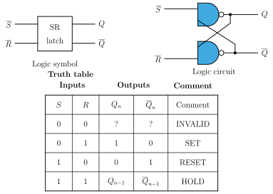
The simplest flip-flop is the SR latch: two inputs S and R, two complementary outputs and , with the state read from . An active-LOW SR latch is built from two cross-coupled NAND gates whose active-low inputs are and (Figure 10.5.3). Its four cases are:
- drives both and to 1, which contradicts the requirement that the outputs be complementary — the INVALID state;
- forces — SET;
- forces — RESET;
- leaves the output unchanged — HOLD.
Note
In the printed truth table the input columns are headed simply S and R, even though the actual circuit inputs are the active-low and . The truth-table card below reproduces the book's column headings exactly as printed.
Unclocked SR flip-flop (active-HIGH NAND latch)
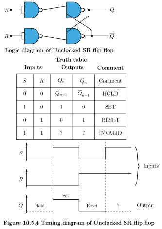
Inserting inverters at the inputs of the cross-coupled NAND latch produces an unclocked SR flip-flop, also called an active-HIGH NAND latch (Figure 10.5.4). It now responds to active-HIGH S and R:
- S=0, R=0 — the latch does not respond, outputs HOLD;
- S=1, R=0 — SET ();
- S=0, R=1 — RESET (), and note that follows S;
- S=1, R=1 — both internal lines go to 0 and force and both HIGH — INVALID/FORBIDDEN.
Clocked SR flip-flop
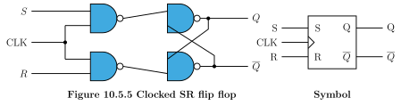
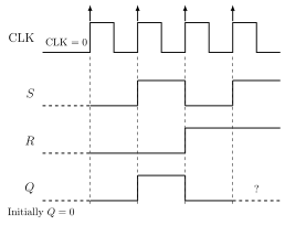
An SR latch is asynchronous: its output can change at any time the inputs change. Adding an enable/clock (CLK) input makes it synchronous — it now acts on its S,R inputs only while CLK is HIGH (Figure 10.5.5). When CLK=1 the four S,R combinations give HOLD, SET, RESET and INVALID exactly as in the unclocked SR flip-flop. When CLK=0 the output holds its previous state for any S,R, so the clock effectively works as an ENABLE. (The timing diagram for the clocked SR flip-flop is printed on the following page without its own figure number.)
From here on, unless stated otherwise, only the clocked versions of the D, JK and JK Master-Slave flip-flops are discussed.
D flip-flop
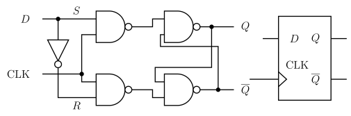
The SR flip-flop's INVALID state (S=R=1) is unwanted. Placing a NOT gate between the S and R inputs guarantees they are always complementary and converts the SR flip-flop into a Data or D flip-flop: data is applied at the single D input and the output simply follows D (Figure 10.5.6). With CLK=0 the output holds; with CLK=1 the output takes the value of D (D=0 → Reset, D=1 → Set).
JK flip-flop
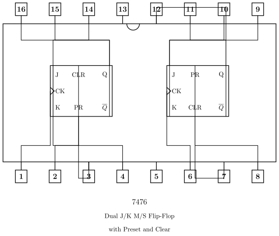
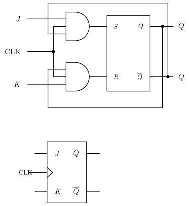
Converting SR to D removes the INVALID state but also loses the useful HOLD condition. The JK flip-flop restores all four behaviours and is the most versatile and widely used flip-flop; commercially it is available as the dual JK flip-flop IC 7476 (Figure 10.5.7). A JK flip-flop is essentially an SR flip-flop in which J is ANDed with to feed S and K is ANDed with to feed R, i.e. and (Figure 10.5.8). With CLK=1:
- J=0, K=0 — HOLD;
- J=0, K=1 — RESET;
- J=1, K=0 — SET;
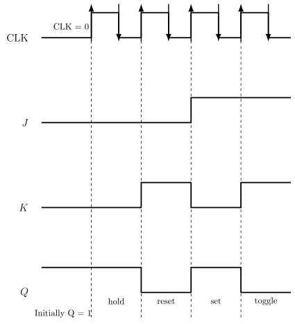
- J=1, K=1 — TOGGLE (the output goes to its complementary state, e.g. becomes ). The full derivation, including the intermediate S and R columns, is tabulated below and the behaviour is drawn in Figure 10.5.9.
Race-around condition
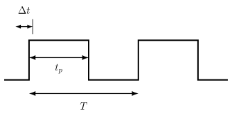
While CLK is HIGH, a JK flip-flop with J=K=1 is in toggle mode. Because the outputs feed back to the inputs, the state can change more than once during a single HIGH interval: after a delay equal to the propagation delay through the gate chain the output complements, and if the clock is still HIGH it complements again after another . Thus for the ON-time of the clock pulse the output keeps flipping between 0 and 1, and its final value at the end of the pulse is uncertain — this is the race-around condition. It disappears if the propagation delay is made longer than the pulse ON-time; since real ICs have very small propagation delays, a Master-Slave arrangement is used instead.
The Master-Slave JK flip-flop …
Drawn by us to help you understand the concept clearly, and verified to make sure it's accurate. For exams, practice from your textbook's own diagram.
Figure 10.5.1 draws a sequential circuit as a combinational-logic block whose outputs are fed back through a memory element into its own inputs. The memory element storing the past state is what gives the circuit its memory and distinguis …

Drawn by us to help you understand the concept clearly, and verified to make sure it's accurate. For exams, practice from your textbook's own diagram.
Figure 10.5.2(a) shows the shape of an ideal clock: a periodic square wave that provides the timing reference synchronizing every memory element in a sequential circuit. What to notice: its equal HIGH and LOW levels and fixed period make this square wave the timing reference that keeps ever …
Drawn by us to help you understand the concept clearly, and verified to make sure it's accurate. For exams, practice from your textbook's own diagram.
Figure 10.5.2(b) labels one clock pulse: the rising (leading) edge where it goes LOW→HIGH, the flat level state while it is HIGH, and the falling (trailing) edge where it returns HIGH→LOW. Edge-trig …
A flip-flop is a bistable multivibrator with two stable states that stores one bit of data (a 0 or a 1). It holds its state indefinitely until an external input changes it, and provides two complementary outputs and . Flip-flops are the basic memor …
Drawn by us to help you understand the concept clearly, and verified to make sure it's accurate. For exams, practice from your textbook's own diagram.
Figure 10.5.3 gives the active-LOW SR latch: a logic symbol (inputs , ; outputs , ) and a logic circuit of two cross-coupled NAND gates. It shows how the SET, RESET, HOLD and INVALID condi …
The book heads the input columns S and R, although the actual circuit inputs are the active-low and ; the headings are reproduced as printed.
| Inputs — S | Inputs — R | Output | Output | Comment |
|---|---|---|---|---|
| 0 | 0 | ? | ? | INVALID |
| 0 | 1 | 1 | 0 | SET |
Drawn by us to help you understand the concept clearly, and verified to make sure it's accurate. For exams, practice from your textbook's own diagram.
Figure 10.5.4 shows the unclocked SR flip-flop — a cross-coupled NAND latch with inverters added at the S and R inputs — together with its timing diagram, which marks the Hold, Set, Reset and the uncertain ( …
| S | R | Comment | ||
|---|---|---|---|---|
| 0 | 0 | HOLD | ||
| 1 | 0 | 1 | 0 | SET |
Drawn by us to help you understand the concept clearly, and verified to make sure it's accurate. For exams, practice from your textbook's own diagram.
Figure 10.5.5 shows the clocked SR flip-flop: the S and R signals are gated with the clock before reaching the cross-coupled output NAND gates, so the flip-flop responds only while CLK is HIGH. Th …
Drawn by us to help you understand the concept clearly, and verified to make sure it's accurate. For exams, practice from your textbook's own diagram.
This timing diagram (printed with Figure 10.5.5 but without its own number) plots CLK, S, R and , showing that updates only during the HIGH intervals of the clock and marking the uncertain ou …
Here X = any input state.
| CLK | S | R | Comment | ||
|---|---|---|---|---|---|
| 1 | 0 | 0 | HOLD | ||
| 1 | 1 | 0 | 1 | 0 | SET |
| 1 | 0 | 1 | 0 | 1 | RESET |
| 1 | 1 | 1 | ? | ? | INVALID |
Drawn by us to help you understand the concept clearly, and verified to make sure it's accurate. For exams, practice from your textbook's own diagram.
Figure 10.5.6 shows the D flip-flop, formed by placing a NOT gate between the S and R inputs of an SR flip-flop so the two are always complementary. Data at the D input is transferred to on the clock; the symbol shows a single D input, a '> …
Drawn by us to help you understand the concept clearly, and verified to make sure it's accurate. For exams, practice from your textbook's own diagram.
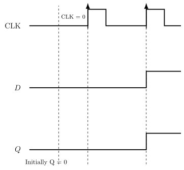
This unnumbered timing diagram (printed with the D flip-flop on the next page) plots CLK, D and , illustrating that simply follows the level of D at the clock edge. Reading the pattern: at each clock the output takes whatever level D holds, so the D flip-flop transfers and …
Here X = any input state.
| CLK | D | Comment | ||
|---|---|---|---|---|
| 0 | X | Hold |
Drawn by us to help you understand the concept clearly, and verified to make sure it's accurate. For exams, practice from your textbook's own diagram.
Figure 10.5.7 gives the functional pin-out of the IC 7476, a 16-pin dual JK master-slave flip-flop with Preset (PR) and Clear (CLR) inputs. Only the pin and function layout is reproduced here, drawn afresh from the pin facts; the …
Drawn by us to help you understand the concept clearly, and verified to make sure it's accurate. For exams, practice from your textbook's own diagram.
Figure 10.5.8 shows the clocked JK flip-flop: J is ANDed with and K with (together with the clock) to feed the internal S and R inputs, giving and . The symbol has J, K, a '>' …
The JK flip-flop is an SR flip-flop whose S and R inputs are gated by the outputs: and . This feedback removes the SR flip-flop's invalid state and adds …
Here X = any input state.
| CLK | J | K | Comment | ||||||
|---|---|---|---|---|---|---|---|---|---|
| 0 | X | X | X | X | X | X | HOLD | ||
| 1 | 0 | 0 | 0 | 1 | 0 | 0 | HOLD | ||
| 1 | 0 | 0 | 1 | 0 | 0 | 0 | HOLD | ||
| 1 | 0 | 1 | 0 | 1 | 0 | 0 | 0 | 1 | RESET |
| 1 | 0 | 1 | 1 | 0 | 0 | 1 | 0 | 1 | RESET |
| 1 | 1 | 0 | 0 | 1 | 1 | 0 | 1 | 0 | SET |
| 1 | 1 | 0 | 1 | 0 | 0 | 0 | 1 | 0 | SET |
Drawn by us to help you understand the concept clearly, and verified to make sure it's accurate. For exams, practice from your textbook's own diagram.
Figure 10.5.9 plots CLK, J, K and for a clocked JK flip-flop and labels the four output behaviours — hold, reset, set and toggle — under successive clock intervals. Reading the pattern: with J=K=0 the output holds, J=0/K=1 resets, J=1/K=0 sets, and J=K=1 toggles to its complement e …
In a clocked JK flip-flop with J=K=1, the output can toggle more than once while the clock stays HIGH, because the outputs feed back to the inputs. After each propagation delay the output complements, so over the pulse ON-time it oscillates between 0 and 1 and its final value is uncertain. This is the race-around cond …
Drawn by us to help you understand the concept clearly, and verified to make sure it's accurate. For exams, practice from your textbook's own diagram.
This unnumbered timing detail (printed with the race-around discussion) marks the small delay , the pulse ON-time and the full period , illustrating how the JK output can flip re …
Drawn by us to help you understand the concept clearly, and verified to make sure it's accurate. For exams, practice from your textbook's own diagram.
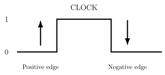
This unnumbered figure marks the positive edge (LOW→HIGH) and negative edge (HIGH→LOW) of a clock pulse, and explains that in the Master-Slave arrangement the positive edge drives the Master while …
Drawn by us to help you understand the concept clearly, and verified to make sure it's accurate. For exams, practice from your textbook's own diagram.
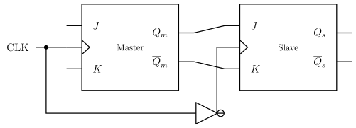
Figure 10.5.10(a) shows the Master-Slave JK flip-flop as a Master JK stage feeding a Slave JK stage; the Slave's clock is inverted so it triggers on the opposite edge, and the Slave outpu …
Drawn by us to help you understand the concept clearly, and verified to make sure it's accurate. For exams, practice from your textbook's own diagram.
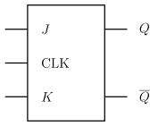
Figure 10.5.10(b) is the single-block logic symbol of the JK Master-Slave flip-flop, with inputs J, CLK, K and outputs , . What to notice: the single '>' clock and the complementary outputs , hide the internal master and slave stages; this …
Drawn by us to help you understand the concept clearly, and verified to make sure it's accurate. For exams, practice from your textbook's own diagram.
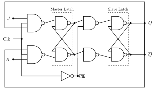
Figure 10.5.10(c) draws the full NAND-gate realization, with the master latch and slave latch highlighted and the clock inverted () to the slave stage, so data passes from maste …
Drawn by us to help you understand the concept clearly, and verified to make sure it's accurate. For exams, practice from your textbook's own diagram.
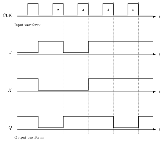
Figure 10.5.11 plots the numbered clock pulses with the J and K inputs and the output, showing the master responding at the rising edge and the slave delivering the final output at t …
Drawn by us to help you understand the concept clearly, and verified to make sure it's accurate. For exams, practice from your textbook's own diagram.
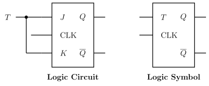
Figure 10.5.12 shows the T flip-flop: the single input T is connected to both the J and K inputs of a JK flip-flop, so with T held HIGH the output toggles once per clock pulse. The symbol has T, CLK …
Drawn by us to help you understand the concept clearly, and verified to make sure it's accurate. For exams, practice from your textbook's own diagram.
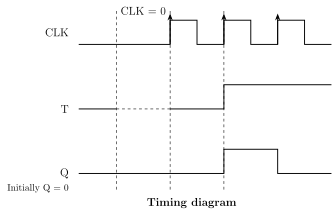
This timing diagram (printed with Figure 10.5.12) plots CLK, T and and shows complementing on successive clock pulses while T = 1. Reading the pattern: with T held HIGH the output flips to its complement on every clock pulse, so the T flip-flop divides the cloc …
Here X = any input state.
| CLK | T | State | |
|---|---|---|---|
| 0 | X | No change | |
| 1 | 0 | No change |